Shi Ming, Chen Ping, Zhao De-Gang, Jiang De-Sheng, Zheng Jun, Cheng Bu-Wen, Zhu Jian-Jun, Liu Zong-Shun, Liu Wei, Li Xiang, Zhao Dan-Mei, Wang Qi-Ming, Liu Jian-Ping, Zhang Shu-Ming, Yang Hui. Thin film micro-scaled cold cathode structures of undoped and Si-doped AlN grown on SiC substrate with low turn-on voltage* . Chinese Physics B, 2015, 24(5): 057901
Permissions
Thin film micro-scaled cold cathode structures of undoped and Si-doped AlN grown on SiC substrate with low turn-on voltage*
Shi Minga)†, Chen Pinga)†, Zhao De-Ganga)‡, Jiang De-Shenga), Zheng Juna), Cheng Bu-Wena), Zhu Jian-Juna), Liu Zong-Shuna), Liu Weia), Li Xianga), Zhao Dan-Meia), Wang Qi-Minga), Liu Jian-Pingb), Zhang Shu-Mingb), Yang Huib)
State Key Laboratory on Integrated Optoelectronics, Institute of Semiconductors, Chinese Academy of Sciences, Beijing 100083, China
Key Laboratory of Nanodevices and Applications, Suzhou Institute of Nano-tech and Nano-bionics, Chinese Academy of Sciences, Suzhou 215123, China
*Project supported by the National Natural Science Foundation of China (Grant Nos. 61474110, 61377020, 61376089, 61223005, and 61176126), the Open Project of the Key Laboratory of Nano-devices and Applications, China (Grant No. 13ZS04), and the National Science Fund for Distinguished Young Scholars, China (Grant No. 60925017).
Abstract
The field emission characteristics of the AlN thin films with micro-scaled cold cathode structures are tested in the high vacuum system. The aluminum nitride (AlN) thin films with a thickness of about 100 nm are prepared on the n-type 6H-SiC (0001) substrate at 1100 °C by metal organic chemical vapor deposition (MOCVD) under low pressure. The I– V curves and surface micro-images of undoped and Si-doped AlN films are investigated. From the I– V and Fowler–Nordheim plots, it can be seen that the Si-doped AlN shows better field emission characteristics compared with the undoped AlN sample. The obtained turn-on field is 6.7 V/μm and the maximum emission current density is 154 mA/cm2 at 69.3 V for the Si-doped AlN film cathode after proper surface treatment. It is proposed that the relatively low electric resistivity of Si-doped AlN films is significant for electron migration to the surface region, and their rougher surface morphology is beneficial to a higher local electric field enhancement for the field emission.
Keyword:
79.60.Bm; 79.60.Dp; 79.70.+q; 79.90.+b; AlN; field emission; cold cathode; negative electron affinity
III– V nitrides have been widely investigated due to their wide applications in optoelectronic and microelectronic devices, including solid-state light emitting diodes (LEDs), [1] blue/green laser diodes (LDs), [2] high electron mobility transistors (HEMTs), [3] and solar cells.[4] Moreover, due to its small and even negative electron affinity (NEA), [5– 7] AlN is believed to be a promising candidate material for the cold cathodes and has potential applications in the field of vacuum systems. For materials with negative electron affinity, the electrons can emit freely from the surface to the vacuum. With a moderate voltage applied, a large field emission current can be obtained, which is necessary in many device applications such as field emission displays (FEDs) and high power microwave devices.
There are many studies about the emission characteristics of AlN materials, including thin films and nanostructures. For example, AlN nanotubes, [8] AlN nanoneedles, [9] and AlN nanorod arrays[10] have been studied. For AlN nanotubes the reported turn-on voltage was 4 kV (with the emission current of 10 nA) and the obtained maximum current was 1 μ A. For nanoneedles and nanorod arrays, the obtained turn-on electric fields were 3.1 V/μ m and 8.8 V/μ m, respectively. The corresponding emission current densities were 4.7 mA/cm2 and 23 mA/cm2, respectively. The field emission (FE) characteristics of AlN thin film cold cathodes could be affected by many parameters. Kasu et al. investigated the FE electrons of various kinds of AlN thin films.[11– 14] They studied the ridge-structure of heavily Si-doped AlN, the FE characteristics of AlN with different concentrations of Si dopant and different layer thicknesses, and the application of the AlN field emitter in a field emission display. They found that as the Si-dopant density in AlN increases from 4.6 × 1018 cm− 3 to 2.5 × 1020 cm− 3, the threshold electric field decreases, and the FE current from AlN increases. Besides, an optimum thickness of AlN for field emission may exist. The reported minimum turn-on electric field was 11 V/μ m and the maximum field emission current density was 0.22 A/cm2.
Silicon vacuum channel transistors[15, 16] have drawn much attention in recent years. They can combine the advantages of a vacuum tube and a transistor, and operate at a moderate voltage due to the fact that the distance between the cathode and the anode is only at the nanoscale. On the other side, AlN has good emission characteristics, stable physical and chemical properties, high reliability, and anti-radiation characteristics. It will be very interesting to check the possibility of employing AlN films as the cold cathode in the field emission devices with a nanoscale vacuum channel structure.
In this paper, we study the FE characteristics of undoped and Si-doped AlN films in a cold cathode structure with a short cathode– anode distance. The AlN films are grown on 6H-SiC substrates. It is experimentally demonstrated that Si-doped AlN has an excellent field emission property compared with the undoped AlN. We obtain a low turn-on electric field of 6.7 V/μ m and a maximum emission current density of 154 mA/cm2 for Si-doped AlN. The obtained turn-on electric field is the lowest among the recently reported values for AlN thin films. Such a low value may be closely related to the necessary process of surface treatment.
2. Experimental setup
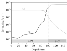
Si-doped and undoped 100-nm-thick AlN thin films were grown directly on n-type 6H-SiC(0001) substrates at 1100 ° C by low-pressure metal organic chemical vapor deposition (MOCVD). Compared to the insulating sapphire substrate, the n-type SiC substrate with high electric conductivity can simplify the device structure and the measurement setup. Meanwhile, the relatively small mismatch of lattice constants and the little difference of thermal expansion constants between SiC and AlN can also benefit the crystal quality of the AlN epitaxial films. The precursors used in MOCVD growth were trimethylaluminum and ammonia (NH3). The flow rates of the precursors were 60 sccm and 500 sccm for trimethylaluminum and ammonia, respectively. The Si-dopant gas was silane (SiH4). The silane flux was 1 sccm for the Si-doped layer. The growth time of the AlN layer was 630 s after the nitridation pretreatment. For the Si-doped AlN film, the Si doping concentration is semi-quantitatively estimated to be in the order of 1018− 1019 cm− 3 according to an un-calibrated second ion mass spectroscopy (SIMS) profile measurement of both the AlN layer and SiC substrate region, as shown in Fig. 1.
Fig. 1. Profiles of silicon and aluminum concentrations for the Si-doped AlN sample measured by SIMS.
The surface morphology of the AlN thin film was measured by atomic force microscopy (AFM).
For the field emission measurement, a 2-μ m-thick SiO2 layer was firstly deposited on the AlN layer in order to insulate the AlN cathode from the Au film anode. A circular hole graph with 1 mm in diameter was patterned in the surface of the SiO2 layer by lithography. This hole was etched through SiO2 to the nitride layer. A parallel Au film anode on sapphire plate was placed on the upper surface of SiO2 to collect the emission electrons. The emission electrons can emit from the AlN cold cathode in this circular hole region to the Au anode. The structure is shown in Fig. 2. The distance between the cathode and the anode was equal to the thickness of the SiO2 layer, i.e., 2 μ m. The real emission area was measured to be ∼ 7.85 × 10− 3 cm2. Because the Al atoms easily react with oxygen in air and then generate oxide on the surface of the AlN layer, processing with the selected acid solution is essential for the proper surface treatment to eliminate the oxide on the AlN surface. The selected acid solution consisted of NH4F, HF, and H2O, and the ratio was about 1:2:3. The etching time was about 10 s. The field emission measurement was performed when the samples were put into a high vacuum system of 1 × 10− 5 Pa. An electric source of a Keithley 2400 was used to apply a bias voltage between the AlN cathode and the Au anode. Although the lowest current of 10 pA can be accurately detected by a Keithley 2400, only the signal above 10 nA is reliable to eliminate the adverse effect of system noise in the I– V measurements. During the field emission measurement, the bias voltage applied to the cold cathode structure was modulated to vary from 0 V to 80 V for undoped AlN and from 0 V to 70 V for Si-doped AlN, with the step of 0.1 V, and the corresponding field emission current was automatically recorded. According to the field emission results, the turn-on voltage and the maximum current density could be obtained, and then the Fowler– Nordheim (F– N) curve was plotted.
Fig. 2. Schematic diagram of micro-scaled field-emission cold cathode structure used in I– V measurements.
3. Results and discussion
Figure 3 shows the FE currents of undoped AlN (black) and Si-doped AlN (red) film samples. The inset shows the magnified I– V curve of the Si-doped AlN near the turn-on voltage region. For the Si-doped AlN, as shown in the inset, the FE current increases slowly with increasing applied bias voltage at first. When the bias voltage is above a certain value, the FE current begins to increase drastically. This bias voltage is the so-called turn-on voltage, which is defined as the voltage corresponding to the current density of 10 μ A/cm2. For the circular emission area of 7.85 × 10− 3 cm2, the corresponding emission current is 7.85 × 10− 8 A. The turn-on voltage is obtained to be 13.4 V. Similarly, the turn-on voltage of undoped AlN is obtained, which is 29.8 V. The turn-on electric field is equal to the turn-on voltage divided by the cathode– anode distance. Here, the turn-on electric field is calculated to be 6.7 V/μ m and 14.9 V/μ m for Si-doped AlN and undoped AlN thin films, respectively. As shown in Fig. 3, the FE current increases more quickly with increasing bias voltage when the bias voltage is larger than the turn-on voltage. For the Si-doped AlN sample, the maximum current is measured to be 1.21 mA at 69.3 V. The maximum FE current density is calculated to be 154 mA/cm2. It is clear that the Si-doped AlN has a better field emission property compared with undoped AlN, i.e., a relatively lower turn-on voltage and a relatively higher FE current. The obtained turn-on electric field is the lowest among the recently reported ones for AlN thin films. We believe that the low turn-on electric field is related to the proper surface treatment and the micro-scaled cathode structure employed. In fact, the Al atoms can easily react with oxygen in air and generate a thin oxide layer on the surface of the AlN layer. This thin oxide layer will act as a barrier for electrons that will be field-emitted to the vacuum. As we can easily remove H2O and soluble metal salt generated during the reaction process of the oxide and an acid solution, a processing with a selected acid solution is essential to eliminate the thin oxide layer on the AlN surface and ensure a low turn-on electric field.
It is noted that the field emission properties of the Si-doped AlN films are better than the undoped ones. While it was reported that for a single microtip of the Si emitter, the n-type Si tip has a lower field emission than the p-type one.[17, 18] The higher turn-on voltage is obtained in the n-type Si sample rather than in the p-type one. This phenomenon is opposite to the result reported for AlN. This may be related to the fact that the surface states of the n-type Si emitter tip are negatively charged, which will form a potential barrier against the electron emission. While there is no potential barrier in the tip of the p-type Si. For AlN, however, the surface potential barrier is relatively low and only has a much smaller impact on the electron emission. Actually, even for n-type AlN, in which the surface states are negatively charged and form a potential barrier for electrons, too, the migration of carriers from the deeper region to the surface has a much more significant influence on the field emission characteristics than the potential barrier induced by the surface states. AlN has a much larger band gap and normally a relatively higher electrical resistivity, the increase of electron concentration in the surface region by carrier migration from the deeper region to the surface is difficult, which may become a significant factor to hinder the field emission. In fact, for undoped AlN, its electric resistivity is very high, there are not so many electrons migrating to the surface during the process of field emission. As a result, it leads to a higher turn-on field and a much smaller emission current compared to the Si-doped AlN film.
Fig. 3. Field emission current of undoped AlN (black) and Si-doped AlN (red) film samples as a function of the applied bias voltage. The inset shows the I– V curve of Si-doped AlN near the turn-on voltage region (marked by an arrow).
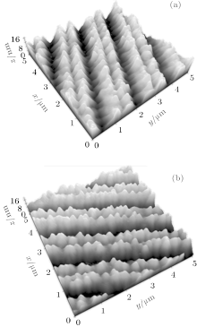
Figures 4(a) and 4(b) show the AFM surface images of the undoped and the Si-doped 100-nm-thick AlN single layers, respectively. From the AFM microimages, the root mean square roughness of undoped AlN and Si-doped AlN is calculated to be 3.377 nm and 3.855 nm, respectively. The surface of the Si-doped AlN film is rougher than that of the undoped AlN film. From the surface morphology of the AlN layers, many aligned ridge tips can be observed. These tips indicate that a three-dimensional (3D) growth mode is dominant during the epitaxial growth of AlN films. The film growth is ended before the islands begin to grow laterally and coalesce. Thus, a step structure on the surface, resulting from a two-dimensional (2D) step-flow growth mode, cannot be obtained for these very thin 100-nm-thick AlN layers. In fact, a kind of periodic structure which looks like an orderly alignment of double lines of densely-distributed hillocks is observed on the surfaces of both samples. Considering the low migration rate of Al adatoms on the surface and the small thickness of the AlN layer, the generation of this periodic structure on the sample surface can be speculated to be related mainly with the inherent step-like microstructure in the surface morphology of the SiC substrate. The surface of the SiC substrate used in MOCVD growth has a miscut orientation relative to the 〈 0001〉 direction. For the Si-doped AlN, these tips have been described as a ridge structure by Kasu.[12] The ridge structure is partly enhanced by the facet growth in the Si-doped AlN. During the AlN growth, Si atoms stabilize facets in the thermal equilibrium state. For the Si-polar SiC (0001) substrate surface, the Al-terminated polar AlN layer will grow on the substrate. During growth, N dangling bonds appear on facets and the and the (0001) planes have an angle of 61° . The Si-dopant atoms form very stable Si– N bonds and prevent Al atoms from adsorption to N atoms. Thus the facets are stabilized. As a result, the ridge structure is formed and a relatively rough surface is obtained. Therefore, the surface roughness of the Si-doped AlN is larger than that of the undoped AlN.
Fig. 4. Atomic force surface micro-images (5 μ m × 5 μ m) of (a) undoped AlN and (b) Si-doped AlN films grown on SiC substrate.
Even though the surface structures of an orderly alignment of double line ridges are similar to each other in undoped and Si-doped AlN samples, the different roughness will still play an important role in field emission characteristics. In principle, when local field-enhancing nanostructures such as pyramid-like tip structures formed by the densely-distributed hillocks are present, the emitter’ s effective field will be enhanced with an enhancement factor β . A larger roughness value will lead to a higher electric field enhancement factor and a better FE property. That is to say, when the same bias voltage is applied, electrons are much easier to emit from the Si-doped AlN surface than from the undoped AlN one.
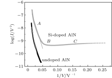
Figure 5 shows the Fowler– Nordheim plots, i.e. log(I/V2) vs. (1/V) plots, for undoped and Si-doped AlN film samples. Under the high voltage, in the F– N plots of both undoped and Si-doped AlN, the curves can be fitted by straight lines with negative slopes (green line for undoped AlN and blue line for Si-doped AlN). It is known that in electric field-induced electron emission processes, the individual electrons can escape by Fowler– Nordheim tunneling in various circumstances. The Fowler– Nordheim equation can well describe the electron tunneling through a rounded triangular barrier created at the material surface when a very high electric field is applied. According to the F– N theory, the slope of a log (I/V2)– 1/V curve may be given as
where β is the electric field enhancement factor, and φ is the work function of AlN. Therefore, the absolute value of k is proportional to the ratio of − φ 3/2 to β . The k can be obtained from the F– N plot. It is known that a low work function and a high enhancement factor are beneficial for obtaining a large FE current. That is to say, a cold cathode with a low absolute value of k is expected to have excellent FE properties. It is found from Fig. 5 that under the application of high bias voltage, log(I/V2) and (1/V) have an approximately linear relationship, demonstrating that in this voltage region, the electron F– N tunneling mechanism is dominant for the field emission of electrons. The absolute value of the slope of the Si-doped AlN F– N plot (k = − 76) is lower than that of the undoped AlN (k = − 116). According to the above analysis, there are two reasons for the difference in k. Firstly, the Fermi level is lifted for the Si doped AlN due to the n-type dopant of silicon. Consequently, the work function of the Si-doped AlN decreases compared to that of the undoped AlN. Secondly, as shown in Fig. 4, the Si-doped AlN has a larger electric field enhancement factor than the undoped AlN, which is due to its rougher surface.
Fig. 5. log (I/V2) vs. 1/V curves (F– N plots) of undoped (black) and Si-doped (red) AlN, and the linear fitting to the high voltage parts of these curves.
As shown in Fig. 5, we separate log (I/V2) vs. (1/V) plot of the Si-doped AlN sample into three sections (A, B, and C) depending on the applied voltage bias. There are mainly two mechanisms of electron emission, i.e., the field-induced emission mechanism and the thermionic emission mechanism, [19] exhibiting very different bias voltage dependences of the emission current. When a small bias voltage is applied to the AlN sample, log (I/V2) almost remains a constant as 1/V decreases, which corresponds to region C of the curve. The field emission current is too low to compare with the thermionic emission current in this low voltage range, the thermionic emission mechanism is dominant in this region. Along with the increase of the bias voltage, the field emission current may rise to the same order of magnitude with the thermionic emission current. The emission currents due to these two mechanisms mix together and a round curve appears in the plot, as shown in region B. When the bias voltage increases to a high value, the log (I/V2) vs. (1/V) curve has an approximately linear relationship, corresponding to region A. A straight line with negative slope can fit this part of the curve very well, which indicates that the field emission mechanism plays a dominant role in the electron emission process. For the undoped AlN sample, the thermionic emission current is too small to be effectively distinguished from the equipment noise and thus cannot be displayed in Fig. 4.
4. Conclusion
The field emission properties and surface micro-images of undoped AlN (u-AlN) and Si-doped n-AlN films grown on n-typed SiC substrate were experimentally investigated. The obtained turn-on electric field was 6.7 V/μ m and 14.9 V/μ m for Si-doped AlN and undoped AlN thin films, respectively. We speculate that the lowest turn-on electric field of Si-doped AlN among the recent reports may be related to the proper surface treatment. The obtained maximum emission current was 1.21 mA at 69.3 V. Considering the emission area of the circular aperture of the AlN sample, the maximum FE current density was calculated to be 154 mA/cm2. From the I– V and Fowler– Nordheim plots, it can be seen that the Si-doped AlN shows better field emission characteristics compared with the undoped AlN sample. The differences between these two types of AlN samples were theoretically analyzed in detail. On one hand, much more electrons are supplied to the surface and emit from the surface to the vacuum for the Si-doped AlN sample. On the other hand, the different surface morphologies accompanied with different magnitudes of field enhancement factors also contribute to the difference of field emission characteristics between the two types of AlN samples.
TondareV N, BalasubramanianC, ShendeS V, JoagD S, GodboleV P, BhoraskarS V and BhadbhadeM2002Appl. Phys. Lett. 804813DOI:10.1063/1.1482137[Cited within:1][JCR: 3.794]
... V nitrides have been widely investigated due to their wide applications in optoelectronic and microelectronic devices, including solid-state light emitting diodes (LEDs),[1] blue/green laser diodes (LDs),[2] high electron mobility transistors (HEMTs),[3] and solar cells ...
1
1994
0.71
0.0
... V nitrides have been widely investigated due to their wide applications in optoelectronic and microelectronic devices, including solid-state light emitting diodes (LEDs),[1] blue/green laser diodes (LDs),[2] high electron mobility transistors (HEMTs),[3] and solar cells ...
1
2013
1.552
0.0
... V nitrides have been widely investigated due to their wide applications in optoelectronic and microelectronic devices, including solid-state light emitting diodes (LEDs),[1] blue/green laser diodes (LDs),[2] high electron mobility transistors (HEMTs),[3] and solar cells ...
1
2013
1.148
1.2429
... [4] Moreover, due to its small and even negative electron affinity (NEA),[5#cod#x2013 ...
1
1998
3.794
0.0
... [4] Moreover, due to its small and even negative electron affinity (NEA),[5#cod#x2013 ...
1
1994
3.794
0.0
1
2000
2.112
0.0
... 7] AlN is believed to be a promising candidate material for the cold cathodes and has potential applications in the field of vacuum systems ...
1
2002
3.794
0.0
... For example, AlN nanotubes,[8] AlN nanoneedles,[9] and AlN nanorod arrays[10] have been studied ...
1
2004
3.794
0.0
... For example, AlN nanotubes,[8] AlN nanoneedles,[9] and AlN nanorod arrays[10] have been studied ...
1
2005
3.794
0.0
... For example, AlN nanotubes,[8] AlN nanoneedles,[9] and AlN nanorod arrays[10] have been studied ...
1
2000
3.794
0.0
... [11#cod#x2013 ...
1
2001
3.794
0.0
... [12] The ridge structure is partly enhanced by the facet growth in the Si-doped AlN ...
1
2001
3.794
0.0
1
2004
3.794
0.0
... 14] They studied the ridge-structure of heavily Si-doped AlN, the FE characteristics of AlN with different concentrations of Si dopant and different layer thicknesses, and the application of the AlN field emitter in a field emission display ...
1
2012
31.17
0.0
... Silicon vacuum channel transistors[15,16] have drawn much attention in recent years ...
1
2012
3.794
0.0
... Silicon vacuum channel transistors[15,16] have drawn much attention in recent years ...
1
2005
0.0
0.0
... [17,18] The higher turn-on voltage is obtained in the n-type Si sample rather than in the p-type one ...
1
2000
1.267
0.0
... [17,18] The higher turn-on voltage is obtained in the n-type Si sample rather than in the p-type one ...
1
2000
3.794
0.0
... , the field-induced emission mechanism and the thermionic emission mechanism,[19] exhibiting very different bias voltage dependences of the emission current ...
Thin film micro-scaled cold cathode structures of undoped and Si-doped AlN grown on SiC substrate with low turn-on voltage*
[Shi Minga)†, Chen Pinga)†, Zhao De-Ganga)‡, Jiang De-Shenga), Zheng Juna), Cheng Bu-Wena), Zhu Jian-Juna), Liu Zong-Shuna), Liu Weia), Li Xianga), Zhao Dan-Meia), Wang Qi-Minga), Liu Jian-Pingb), Zhang Shu-Mingb), Yang Huib)]


 , Jiang De-Sheng