Room temperature ferromagnetism in un-doped amorphous HfO2 nano-helix arrays*
[Xie Qian, Wang Wei-Peng, Xie Zheng, Zhan Peng, Li Zheng-Cao, Zhang Zheng-Jun† ]
]
]
 |


†Corresponding author. E-mail: zjzhang@tsinghua.edu.cn
*Project supported by the National Natural Science Foundation of China (Grant Nos. 51372135 and 61176003) and the Tsinghua University Initiative Scientific Research Program, China.
Amorphous HfO2 nano-helix arrays with different screw pitches were fabricated by the glancing angle deposition technique. Room temperature ferromagnetism was achieved in this undoped amorphous HfO2 nanostructure, which is attributed to singly charged oxygen vacancies. The different magnetic behavior and photoluminescence in flat film and nano-helix arrays originate from the distinction of defect components. This study could facilitate the understanding of ferromagnetism origin in undoped HfO2, it also suggests a possible way to alter the intrinsic defects in amorphous HfO2.
Generally speaking, cations with partially filled d or f shells are required to realize the ferromagnetic order in oxide materials. Hafnium oxide (HfO2) without doping by ferromagnetic ions was once accepted as a diamagnetic material. However, the discovery of room temperature ferromagnetism in pure monoclinic HfO2 thin films[1] in 2004 came as a surprise and greatly challenged our basic understanding of the origin of the ferromagnetism. Subsequently, intensive attention was focused on various oxides, such as HfO2, TiO2, ZnO, and In2O3, due to their theoretically predicted high Curie temperatures and potential applications as spintronic materials.[2– 4] Although some researchers have ascribed the ferromagnetism to the doped ferromagnetic cations[5, 6] or contaminations, [7, 8] the ferromagnetic phenomenon in pure oxides has been finally observed in a broad spectrum of materials and the evidence obtained leaves little doubt about its existence.[9] The high sensitivity of the magnetic properties dependent on the fabrication conditions and the difficulties in explaining the phenomenon with known models led scientists to conclude that various defect states may play a major role in these systems.[10, 11] Intrinsic defects, especially cation vacancies and oxygen vacancies, have been considered as the origin of this unexpected magnetic behavior, [12– 16] however, there is no consistent conclusion about the specific mechanism.
Theoretical research has pointed out that tremendously high concentrated defects with a magnetic charge configuration are required for magnetism generation.[17] Compared to crystalline materials, amorphous materials have a much higher intrinsic defect concentration owing to the lack of a three-dimensional long-range order.[18] Meanwhile, nanostructured films are supposed to contain more intrinsic defects than the conventional ones due to their inherently porous nature and enormously huge specific surfaces.[19, 20] Since the unexpected ferromagnetism was first reported in HfO2, it may be helpful to understand the origin of ferromagnetism by focusing on amorphous HfO2 nanostructures. In particular, there is an average decrease in the formation energy of oxygen vacancies in amorphous HfO2 according to theoretical calculations, [21] which indicates that a higher oxygen vacancy concentration could be achieved. In addition, the overall electronic structure of HfO2 is not so sensitive to the amorphous structure details due to the short-range order presented over several molecular dimensions, [21] which allows the application of electronic theory and models for crystalline HfO2.
In this paper, the glancing angle deposition (GLAD) technique is utilized to produce HfO2 thin films with pre-designed nanostructures, [22, 23] which is ideally suited for the introduction of large defect concentrations. The room temperature ferromagnetism properties of these nanostructured films are investigated and the mechanism is discussed.
Amorphous HfO2 nano-helix arrays were fabricated with the GLAD technique using electron beam evaporation. The base pressure was lower than 2× 10− 4 Pa. Si (001) substrates were ultrasonically cleaned in acetone, ethanol, and de-ionized water baths in sequence. An HfO2 ceramic target with a purity of 99.99% was used as the evaporation source. The deposition angle α (defined as the angle between the trajectory of the incident beam vapor flux and the surface normal of the substrate) was set at ∼ 85° . By altering the deposition angle and the self-rotation rate, nanostructures with different morphologies were successfully fabricated. A conventional dense flat film deposited at α = 0° , with the same thickness of the nanostructured film, was also prepared for comparison.
The structure and composition of the samples were characterized by using an x-ray diffractometer (XRD, Rigaku Dmax 2500V), a field emission scanning electron microscope (FESEM, JEOL-7001F), a transmission electron microscope (TEM, JEOL 2010), an x-ray photoelectron spectroscopy spectrometer (XPS, Thermo Fisher ESCALAB 250Xi), and induced-coupled-plasma atomic emission spectrum analysis (ICP-AES, ELAN DRC-e). The performance of photoluminescence and the magnetic properties were evaluated by a Raman spectrometer (Horiba Jobin Yvon, LabRAM Aramis, He– Cd Laser, 325 nm) and a superconducting quantum interface device (SQUID, MPMS XL-7), respectively. In order to eliminate unintentional ferromagnetic contamination, bamboo tweezers were used for handling the samples and care was taken to keep the samples away from any ferromagnetic material or metal, such as sample holders, tooling fixtures, and containers.
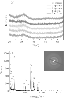
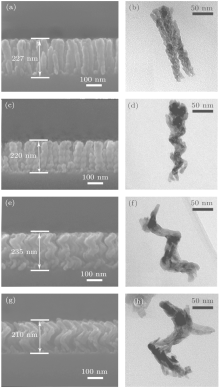
The amorphous phase of the samples is confirmed by XRD and selected area electron diffraction (SAED). As shown in Fig. 1(a), there is no diffraction peak observed in the XRD patterns of the samples. In addition, the SAED images of the nano-helix samples show a diffuse halo, which confirms that the samples are amorphous. The energy dispersive x-ray spectrometry (EDX) result in Fig. 1(b) shows that the sample is mainly HfO2, the signals of Cr and Cu come from the sample holder. The morphologies (SEM and TEM images) of the as-prepared films are shown in Fig. 2. The thickness of these films is around 220 nm, as denoted in the SEM images. Each sample consists of vertically aligned HfO2 nano-helices with a diameter of ca.10– 30 nm. The helix morphology could be retained during the TEM sample preparation. As shown in Figs. 2(a) and 2(b), when the screw pitch is shorter than the diameter of the column, the helical geometry is indistinct. As the pitch increases, the helical geometries of the samples become clearer. There are four spirals, two spirals, and one spiral in Figs. 2(d), 2(f), and 2(h), respectively. The small pitch sample in Fig. 2(b) can be considered to have infinite spirals (∞ ). Thus, the screw pitches of the samples could be determined as 0 nm, 55 nm, 117 nm, and 210 nm along with the decreasing numbers of spirals.
 | Fig. 1. (a) XRD patterns of the as-prepared samples, (b) EDX result with SAED image in the inset. |
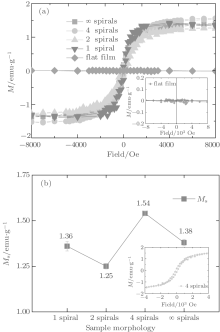
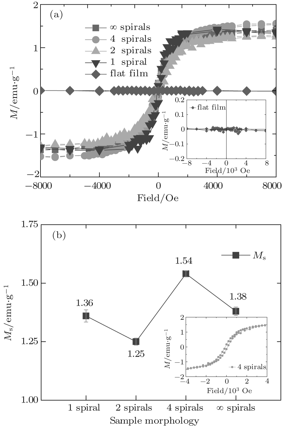
Magnetization of the samples versus the external magnetic field is shown in Fig. 3(a). These samples were measured at 300 K with a maximum applied magnetic field of 8 kOe, and the diamagnetic signals of the substrates and the holders were deducted. It is worth noting that all of the amorphous HfO2 nanostructured films exhibit hysteresis loops, which is a characteristic of ferromagnetic ordering. This is different from the sample without nanostructures, i.e., the HfO2 flat film, which exhibits a diamagnetic property in Fig. 3(a). The saturation magnetizations (Ms) of the samples were determined from the M– H curves and normalized with the Hf mass quantitated by ICP-AES. The Ms– morphology curve is illustrated in Fig. 3(b). As the spiral number increases, Ms fluctuates slightly. The maximum Ms reaches 1.54 emu/g, approximately 5.8× 10− 2 μ B/f.u. (Bohr magneton per formula unit, for HfO2, 1 emu/g≈ 3.77× 10− 2 μ B/f.u.), in the sample with four spirals, which is about two orders of magnitude higher than that in monoclinic HfO2 nanorods (6.7× 10− 4 μ B/f.u.), [24] and three orders of magnitude higher than that in monoclinic HfO2 powder (7× 10− 5 μ B/f.u.).[13] The enhancement of ferromagnetism in this study indicates a coupling effect between the nanostructure and the amorphous state.
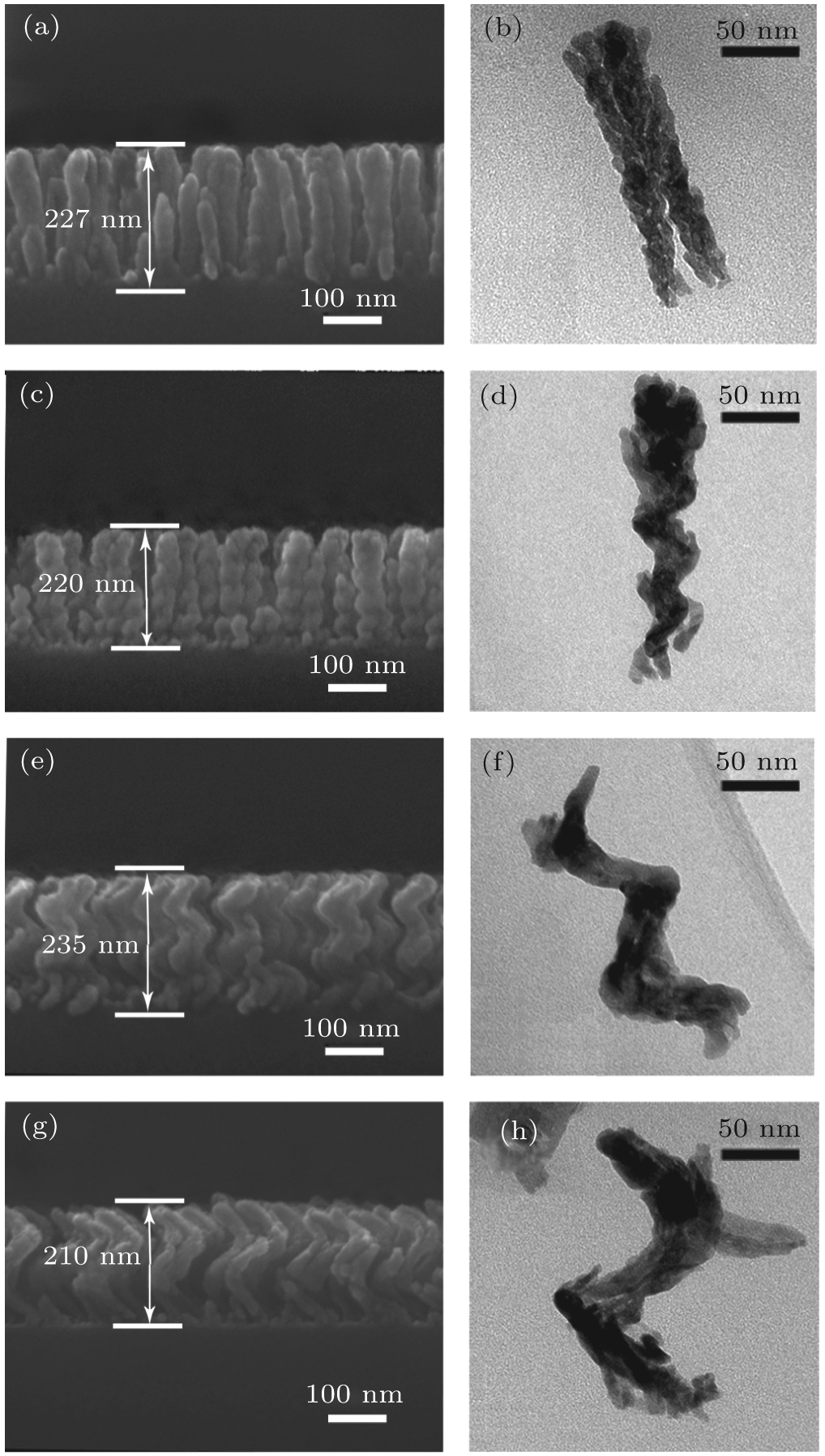 | Fig. 2. SEM images of nano-arrays from side view and TEM images of single nano-column. (a), (b) Sample with ∞ spirals per column; (c), (d) sample with four spirals per column; (e), (f) sample with two spirals per column; (g), (h) sample with one spiral per column. |
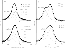
In order to understand the physical origin of room temperature ferromagnetism existing in HfO2 nanostructures, and to confirm that all of the ferromagnetic behaviors come from pure HfO2, XPS measurement was employed. Firstly, the effect of ferromagnetic element contaminations is excluded by XPS results, which is also confirmed by ICP measurement. Deposited in a vacuum environment, the samples are expected to be oxygen deficient. Measuring the profile of the oxygen deficiency states is necessary. Figure 4(a) shows the O 1s spectra of the flat film and the four spiral sample (with maximum Ms). Both spectra have an asymmetric shape and a broad shoulder to the higher binding energy, indicating that several oxygen species are presented in the near surface region. The O 1s spectra are thus fitted by three symmetric Gaussian– Lorentz peaks. The intense peak at about 533.1 eV (1s a) is attributed to the oxygen in stoichiometrical environment. The medium peak located at 533.9 eV (1s b) is related to the loss of oxygen in the sample and associated with the O2− ions in the oxygen-deficient regions. The highest binding energy peak at 534.9 eV (1s c) can be assigned to the near-surface oxygen.[25– 28] The proportion of the stoichiometrical oxygen peak (1s a) is 51.1% in the flat film, and decreases to 45.4% in the four spiral sample, while the oxygen deficiency related peak (1s b) increases from 32.3% to 38.3% in Fig. 4(a). Similar phenomena were also observed in other nano-helix samples, with lower proportion of stoichiometrical oxygen peak (1s a) and higher proportion of oxygen deficiency related peak (1s b). The results indicate that the nanostructures are less stoichiometrical, in other words, they contain more oxygen vacancies than the flat film sample. Figure 4(b) exhibits the XPS spectra of Hf 4f, consisting of two peaks for Hf 4f7/2 and Hf 4f5/2. The binding energies of the samples are higher than those of fully oxidized HfO2, and represent the feature of O-deficient HfO2 film.[29, 30] The higher energy peak should originate from the Hf– O in the vicinity of Hf or Hf, Hf– O bond.[31] The peak of the flat film is narrow and better resolved, consistent with the results of the conventional HfO2.[32– 34] For the nanostructured sample, the peak in Fig. 4(b) is broad with poor resolution, indicating more bonding configurations for the Hf in the nanostructures.[35]
 | Fig. 3. (a) Hysteresis curves of samples measured at room temperature, (b) room temperature Ms versus the sample morphology. |
 | Fig. 4. XPS spectra: (a) O 1s core level spectra and (b) Hf 4f core level spectra of the flat film sample and the four spiral sample. Symbols are for experimental data and the solid lines are fits with Gaussian peaks. |
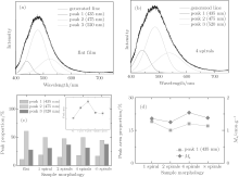
Theoretical studies have suggested that oxygen vacancies can cause an obvious change of the band structure of the host oxides and make a significant contribution to the ferromagnetism.[36, 37] From the previous studies, HfO2 exhibits visible-light photoluminescence (PL) due to the presence of oxygen vacancies, [38, 39] with the emission band energies ranging from 2.9 eV to 4.0 eV depending on the fabrication technique.[38– 41] To confirm the oxygen vacancies indicated by the XPS analysis, room temperature PL studies were performed in our study. Each sample showed a broad PL band covering a large part of the visible spectrum with a maximum situated at 490 nm (2.53 eV), as shown in Fig. 5. This profile suggests an emission mechanism with the participation of several energy levels or light emission centers able to trap electrons within the band gap.
To further explore the emission properties of the HfO2 nanostructure, the PL spectra of the samples are fitted with three Gaussian peaks, i.e., peak 1 located at 435 nm (2.85 eV), peak 2 located at 475 nm (2.61 eV), and peak 3 at 520 nm (2.38 eV), as shown in Figs. 5(a) and 5(b). The locations of the Gaussian peaks are consistent with the calculation and the previous experiment.[42– 44] Peak 1 corresponds to singly charged oxygen vacancies (F+ centers).[45] Peak 2 can be assigned to the excitation electrons jumping from doubly charged oxygen vacancies to singly charged oxygen vacancies.[46] While peak 3 corresponds to neutral oxygen vacancies (Vo0).[45]
The relationship between the peak area proportion and the sample morphology is demonstrated in Fig. 5(c). The data only vary minimally among the nano-helix samples. The pattern of the flat film differs from the others by the smaller proportions of peak 1 and peak 3. Therefore, the distinction of the peak area proportion is ascribed to the defect state difference between the nanostructured films and the flat film. A comparison of the total peak area is plotted in the inset of Fig. 5(c). The emission efficiency of the nanostructured films is higher than that of the flat one, indicating a higher defect density, which is similar to the research on amorphous silicon nanostructures.[47] The intensity of the emission culminates at the two spiral sample. In the four spiral and the ∞ spiral samples, the upper spirals may shelter the lower ones from incident laser photons, which reduces the effective illumination area.
To explore the relationship between ferromagnetism and the defects, we plot the peak 1 area proportion and Ms versus the sample morphology in Fig. 5(d). Comparing the two curves, a (not strictly) positive correlation between Ms and the area proportion of peak 1 can be obtained. However, peak 2 and peak 3 show no evident relationship with Ms, indicating the singly charged oxygen vacancies (F+ centers) involved with the ferromagnetism.
Upon the loss of an O atom, the electron pair remains trapped in the vacancy cavity VO. The electrons associated with defects in oxides have a high dielectric constant, occupy large Bohr orbits, and tend to form an impurity band. By allowing the impurity band to mix with the empty 5d states of hafnium and to transfer a fraction of an electron for each vacancy, the 5d states would therefore in turn polarize the impurity band and provide the necessary ferromagnetic coupling.[1] A basic assumption is that the high charge of the Hf4+ ion tends to polarize the surrounding oxygen shells, and one of the electrons in Vo tends to occupy the neighboring Hf4+ ion and yield Hf3+ and F+ center forming shallow and deep trap states. The locally trapped electron in the F+ center occupying an orbital overlapping with the unpaired electron (5d1) of Hf3+ is proposed as the origin of ferromagnetism in our samples. Thus, the more bonding configurations for the Hf in nanostructures detected by XPS can be also explained.
 | Fig. 5. (a) PL spectra and peak fit of the flat film sample; (b) PL spectra and peak fit of the four spiral sample; (c) peak area proportions of the Gaussian peaks, the inset shows the total PL peak area of each sample; (d) Ms and the peak 1 area proportion versus the sample morphology. |
Amorphous HfO2 nano-helix arrays were successfully fabricated by the glancing angle technique. The magnetic measurements showed that all HfO2 nanostructures exhibit intrinsic room temperature ferromagnetism. The XPS and PL spectra revealed that the origin of the ferromagnetism could be attributed to the singly charged oxygen vacancies (F+ centers). The nano-helix morphology exerts a great impact on the intrinsic defect states and enhances the ferromagnetism greatly. This study has established a correlation of ferromagnetism with the F+ centers in the HfO2 nano-helices and has also helped to gain better insight into the defect engineering of room temperature ferromagnetism in undoped HfO2.
| 1 |
|
| 2 |
|
| 3 |
|
| 4 |
|
| 5 |
|
| 6 |
|
| 7 |
|
| 8 |
|
| 9 |
|
| 10 |
|
| 11 |
|
| 12 |
|
| 13 |
|
| 14 |
|
| 15 |
|
| 16 |
|
| 17 |
|
| 18 |
|
| 19 |
|
| 20 |
|
| 21 |
|
| 22 |
|
| 23 |
|
| 24 |
|
| 25 |
|
| 26 |
|
| 27 |
|
| 28 |
|
| 29 |
|
| 30 |
|
| 31 |
|
| 32 |
|
| 33 |
|
| 34 |
|
| 35 |
|
| 36 |
|
| 37 |
|
| 38 |
|
| 39 |
|
| 40 |
|
| 41 |
|
| 42 |
|
| 43 |
|
| 44 |
|
| 45 |
|
| 46 |
|
| 47 |
|