


Experimental and theoretical study on field emission properties of zinc oxide nanoparticles decorated carbon nanotubes*
[Li Xin† , Zhou Wei-Man, Liu Wei-Hua, Wang Xiao-Li]
, Zhou Wei-Man, Liu Wei-Hua, Wang Xiao-Li]
|
|


†Corresponding author. E-mail: lx@mail.xjtu.edu.cn
*Project supported by the National Natural Science Foundation of China (Grant Nos. 91123018, 61172040, and 61172041) and the Natural Science Foundation of Shaanxi Province, China (Grant No. 2014JM7277).
Field emission properties of zinc oxide (ZnO) nanoparticles (NPs) decorated carbon nanotubes (CNTs) are investigated experimentally and theoretically. CNTs are in situ decorated with ZnO NPs during the growth process by chemical vapor deposition using a carbon source from the iron phthalocyanine pyrolysis. The experimental field emission test shows that the ZnO NP decoration significantly improves the emission current from 50 μA to 275 μA at 550 V and the reduced threshold voltage from 450 V to 350 V. The field emission mechanism of ZnO NPs on CNTs is theoretically studied by the density functional theory (DFT) combined with the Penn–Plummer method. The ZnO NPs reconstruct the ZnO–CNT structure and pull down the surface barrier of the entire emitter system to 0.49 eV so as to reduce the threshold electric field. The simulation results suggest that the presence of ZnO NPs would increase the LDOS near the Fermi level and increase the emission current. The calculation results are consistent with the experiment results.
Carbon nanotubes (CNTs) have been intensively studied in the past two decades due to their great application potentials in electronics and photonics.[1– 3] Especially as the field emission cathode, [4] CNTs have demonstrated great potentials in applications like field emission display (FED) and vacuum microwave devices.[5] Samsung has even demonstrated a five-inch CNT FED, [6] which is possibly one of the few CNT-based devices that are very close to a commercial product. However, emission current low and long term instability are two possibly the main hampers for the real application of the CNTs as field emission cathode besides of the competitive from liquid-crystal display. The CNT field emission mechanism is that electrons can overflow the CNT surface barrier into a vacuum under an external electric field that reduces the barrier height and width. Many research groups tried to modify the CNT surface by doping and adsorption of metal oxides to improve the field emission current.[7, 8] Using nanoparticles to decorate the surface of the CNTs, such as diazonium salt reduction, polymer composites, and Al2O3, could build novel structures to enhance the electron transmission.[9, 10] Some groups have focused on the nanostructures of the ZnO nanoparticles coated on the surface of multi-wall carbon nanotubes (ZnO/CNTs composites).[11– 14] Theoretical research has shown that the electron energy state of the CNT surface is the key factor influencing the emission current and threshold field, because the electron structure of the CNT shows a unique quantum state. Fairchild’ s group, [15] Choi’ s group, [16] and other groups have reported that the composite interface helps the electron overflow from the surface by reducing the work function, and studied the electronic structure, spectral properties, and surface state with the DFT and molecular dynamics method.[17, 18] Liu’ s group[19] reported that Ru nanoparticles improve the emission property of the CNT by reducing the work function and increasing the density of emission sites. However, the surface functional modification makes the CNT emitter tip structure complex, and expressions of the electronic density of state of the emitter surface complicated.
We investigate the field emission property of ZnO and CNT composite structure emitters in experiment and theory. We have tried in situ ZnO NPs decorated CNTs during its growing process to prepare the ZnO– CNT emitter, and tested the field emission properties in the experiment. In view of this complex field emitter, we adopt the Penn– Plummer model to calculate the field emission properties of ZnO– CNT. A DFT model combined with the Penn– Plummer method of the ZnO– CNT structure is built to study the local density of states and the field-emission barrier shape. We provide a new insight for understanding the field emission properties of the CNT composite.
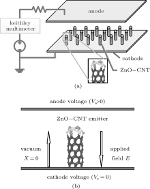
The cathodes were prepared in the following process: first, 10 gram ball milling ZnO nanoparticles were dispersed into a 30 ml terpineol solution, and 4 gram ethyl cellulose was dispersed in the above solution, assisted by the ultrasonic so as to form the composite paste. The composite paste was then heated to 200 ° C, and the ZnO NP layer was printed on the substrate through a screen-printing process. The layer thickness of ZnO NPs was about 10 microns. Before the growth of CNTs, the ZnO NP layer needs to be baked at 540 ° C to remove all of the organic impurities. Second, the substrate with ZnO NP layers was introduced into a quartz tube for the growth of CNTs with a typical catalytic pyrolysis method with FeC32N8H16 (FePc). A typical synthesis process was reported in our previous work.[11, 13] The ZnO NPs decorated CNTs film was prepared and placed on the cathode of the diode configuration field emission test setup, as shown schematically in Fig. 1(a). A uniform electric field is applied to the anode and cathode, and the space between the anode and cathode is fixed at 150 μ m with the spacer. The vacuum level was kept at about 5 × 10− 5 Par during measurements. The anode was an ITO phosphor glass which was purchased (QINHUANGDAO YAOHUA GLASS CO., LTD. P. R. CHINA) and has a size of 10 × 10 mm2, almost the same as that of ZnO NP decorated CNT cathode. The morphology of ZnO NP decorated CNTs was investigated by using a transmission electron microscope (TEM) (JEOL JEM-2010) and a scanning electron microscope (SEM) (S-4800). A Keithley Multimeter 2000 was used as the electrical voltage (V) and emission current (I) measurement.
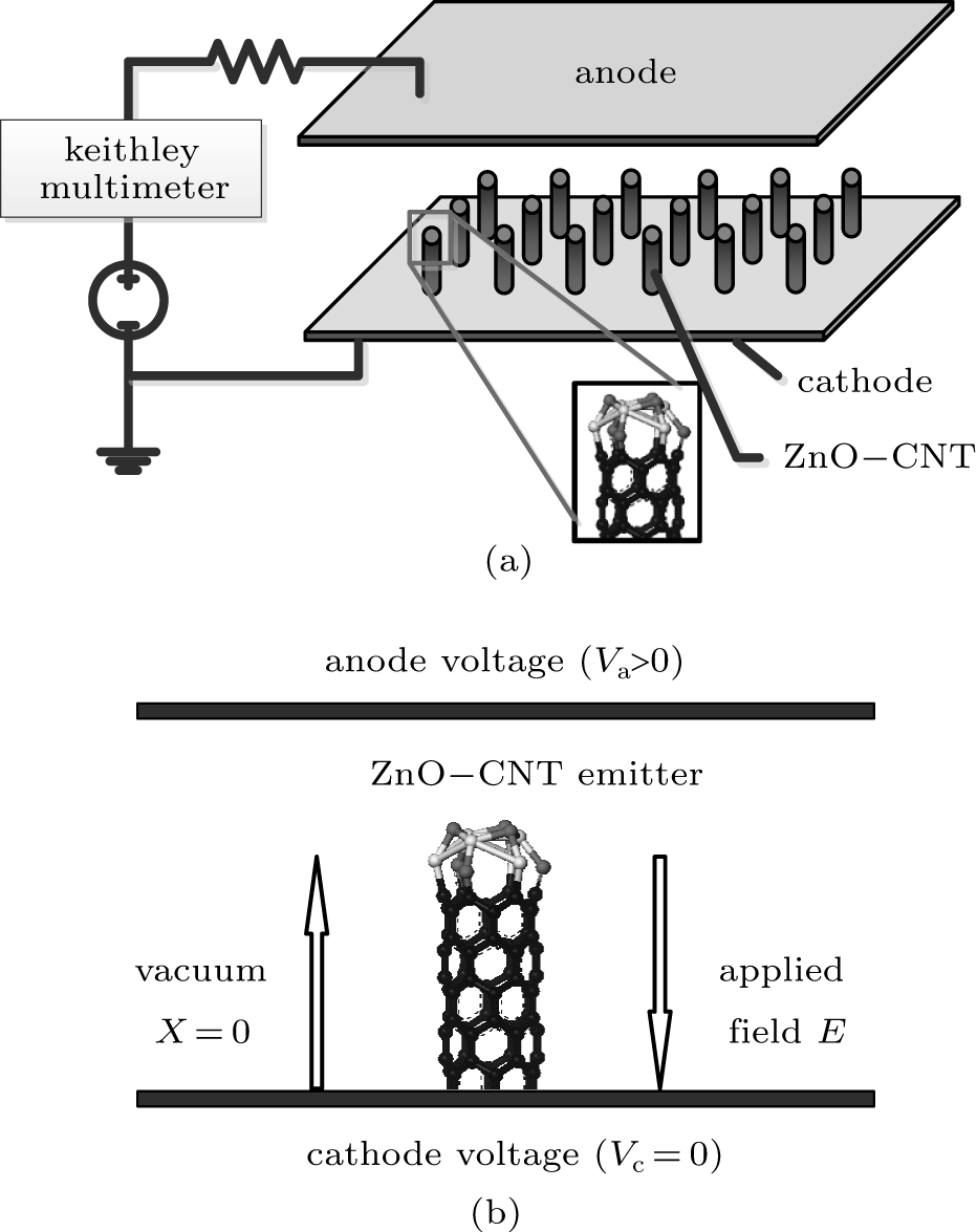 | Fig. 1. (a) Schematic diagram of the experiment setup of the field emission of the ZnO NP decorated CNT cathode with a uniform electric field in the vacuum cavity applied to the anode and cathode. The voltage (V) and emission current (I) are monitored. (b) Schematic diagram of individual ZnO NP decorated CNT (ZnO-CNT) emitter model. |
The Penn– Plummer field emission model[17, 18] is used to investigate the complex field emitter like ZnO NP decorated CNTs and simulate emission current density. The local density of state (LDOS) and the surface electron effective potential Veff of the emission surface are calculated by the first principle calculation software VASP. Individual ZnO NP decorated CNTs (ZnO-CNT) emitter model is shown in Fig. 1(b). The voltage on the anode is positive (Va > 0), the voltage on the cathode is zero (Vc = 0), and the applied field E is from the anode to the cathode. The emitter structure is the ZnO NPs on the top of CNTs that are placed vertically on the cathode. Two kinds of emitters of ZnO NP decorated CNTs (ZnO-CNT) and pure CNT (CNT) are compared to investigate the influence of ZnO on CNTs in field emission.
The SEM and TEM images of the ZnO NP decorated CNTs are shown in Fig. 2. The diameters of CNTs are about 100 nm and ZnO nanoparticles (denoted by the dark dots in white circles) are normally 5– 10 nm. The ZnO NPs are embedded in the wall of CNTs and distribute evenly along the whole side wall of CNTs. ZnO NPs increase the emission active sites on the CNT, [20] so that the electron could emit from not only the top but also the side wall of CNTs. The HRTEM image of a hetero junction between a ZnO NP and CNT is shown in the inset of Fig. 2(b). The ZnO NPs prepared by the catalytic pyrolysis method have a diameter of 5– 10 nm and a lattice spacing of 0.29 nm, which agrees well with the inter-planar distances of a (100) plane of ZnO.
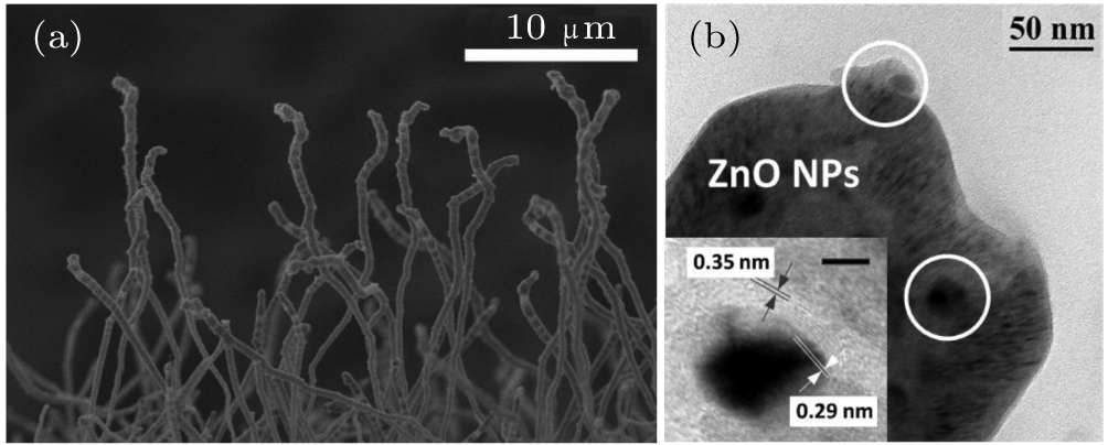 | Fig. 2. SEM and TEM images of ZnO NPs decorated on CNTs. (a) SEM image of ZnO NP decorated CNTs array. (b) HRTEM image of ZnO NPs attached on the top of individual CNT. Inset: an HRTEM image of the white circle zone (scale bar: 5 nm). |
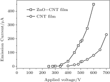
The experimental results of field emission are shown in Fig. 3. The circle curve is from the pure CNT cathode and the square from ZnO-CNT. The threshold voltages of ZnO-CNT and pure CNT emitters are 350 V and 450 V, defined as the voltage when the field emission current is 12 μ A, respectively. Their emission currents at 550 V are 275 μ A and 50 μ A, respectively. The ZnO NP decoration significantly reduces the field emission threshold voltage of the CNT emitter, because the ZnO NPs on the CNTs provide more effective field emission active sites and increase the emission current, as shown in the micro images in Fig. 2. To further confirm that the role of the ZnO NP decoration on the surface of CNT influences the field emission property, the electronic structure and emission mechanism of ZnO-CNT and CNT will be compared.
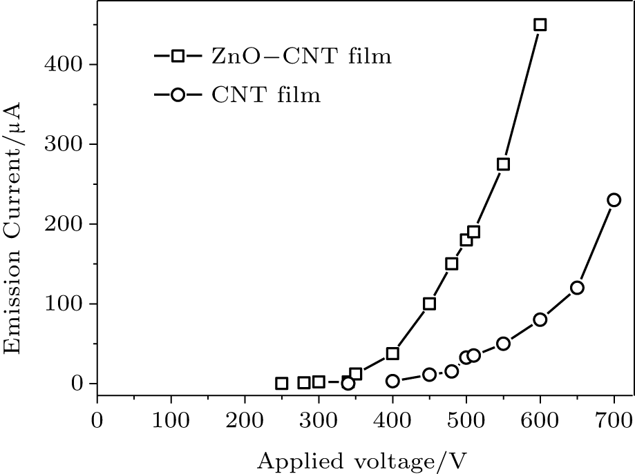 | Fig. 3. Field emission I– V curves of CNT and ZnO NP decorated CNT cathode. The threshold voltage of the ZnO-NP decorated CNT cathode and the pure CNT cathode are 350 V and 450 V, respectively. The field emission current is 12 μ A. |
The Penn– Plummer field emission model is used to analyze the electronic structure and emission mechanism of the ZnO-CNT emitter surface. The emission current density of electrons with energy E is calculated by

where me is the electron effective mass, f (E) is the Fermi– Dirac distribution, S is the area of the surface element, and λ (E) is a slowly varying function of energy, which results from linear fitting of the CNT-ZnO internal surface barrier of the WKB wave function. The D2(E, W(x)) is the probability of electrons overflowing the surface barrier into the vacuum and is defined by the surface barrier function W(x). The schematic diagrams of the first principle of the field emission topology model of ZnO-CNT and CNT are shown in Fig. 4.
 | Fig. 4. Schematic diagram of the topology model of ZnO-CNT and CNT. |
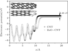
Geometry optimization results show that obvious structure reconstruction occurs on the surface of Zn and C, because of the interaction of Zn– C, Zn– O, and C– O bonds. The surface atomic interaction will significantly modify the height, width, and shape of the surface barrier.[21, 22] After the structure geometry optimization, the surface barrier W(x) of ZnO-CNT and a pure CNT at the equilibrium state are calculated (E = 0) and shown in Fig. 5.
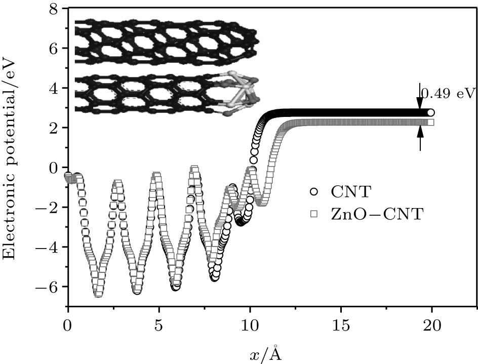 | Fig. 5. Simulation results of CNT-ZnO and pure CNT surface barrier at the equilibrium state. The circles represent the calculated (E = 0) W(x) of pure CNT, and the squares represent ZnO-CNT. |
In Eq. (1), the probability D2(E) is very sensitive to the work function of the emitter material structure. The ZnO-CNT emitter surface will reconstruct because of the competition between Zn– C, Zn– O, and C– O interactions, and the interactions between different atoms play an important role in changing the surface barrier height and shape. The simulated electronic potential W(x) is along the tube axis direction x. The electronic potential valleys correspond to the position of carbon atoms, and the peaks correspond to the center of the carbon hexagonal structure. The circles represent the results of a pure CNT and the squares represent those of a ZnO-CNT. The vacuum barrier of the pure CNT is 0.49 eV higher than that of the ZnO-CNT. It clearly shows that the ZnO NPs on the top of the emitter effectively pull down the surface barrier height of the entire ZnO-CNT system, so that it is easier for electrons to overflow from the surface of ZnO-CNT than from that of the pure CNT. Consequently, the threshold voltage decreases. This is the reason why the field emission threshold voltage of the ZnO-CNT emitter is lower than that of the CNT emitter in experimental curves, as shown in Fig. 3.
The vacuum barrier for an electron overflowing from an emitter surface would incline from squares to triangles under an electric field. However, the electrostatic potential inside the material has not been changed significantly. The larger the electric field, the more obvious the barrier inclines. From Fig. 6 the slope of the red square curve (0.6 V/Å ) is greater than that of the black circle curve (0.3 V/Å ). The applied field further improves the probability of electrons overflowing from the surface barrier into the vacuum.
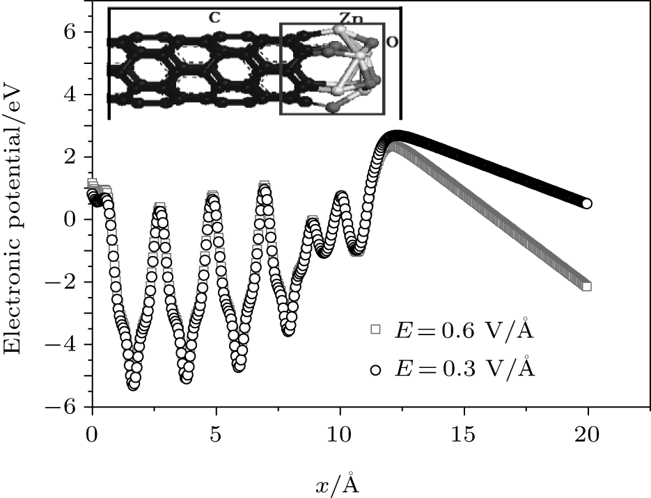 | Fig. 6. Simulation results of the CNT-ZnO emitter surface barrier under different fields. Black circle and red square dots represent calculated W(x) at fields of E = 0.3 V/Å and E = 0.6 V/Å , respectively. |
To investigate the mechanism of the ZnO-CNT field-emission property, a density functional theory (DFT) model combined with the Penn– Plummer method is used to calculate the local densities of states (LDOS) near the Fermi level (Ef = 0), as shown in Fig. 7. The LDOS of the CNT-ZnO is significantly larger than that of the CNT. Because the LDOS near the Fermi level (Ef) contributes most of the emission current, this result suggests that the ZnO-CNT emitter provides more effective emission electrons than the CNT emitter. This is the reason why the emission current from the ZnO-CNT emitter is larger than that from the CNT emitter, as shown in Fig. 3.
 | Fig. 7. DFT simulation results of the LDOS near the Fermi level (Ef = 0 eV). |
To further examine the effects of the surface LDOS and the surface barrier W(x) on the field emission property, calculated LDOS and W(x) were brought into the Penn– Plummer model field emission current equation (Eq. (1)). The I– V curves in the lower field of both CNT-ZnO and pure CNT are calculated and shown in Fig. 8. Since the calculated dots are limited, we can only compare two curves at the lower field. The threshold field of the ZnO-CNT is 0.6 V/Å lower than that of CNT. It fits well with the previous experimental results. Since the emission current increases exponentially with the barrier height reducing in the turn on process, reducing the emitter surface barrier not only affects the threshold electric field, but also the emission current.
 | Fig. 8. Field emission I– V simulation curves of the CNT-ZnO and the pure CNT emitters. The black circles represent pure CNTs, and the red squares represent ZnO-CNT. |
In situ decoration of the CNTs by ZnO NPs has been successfully achieved. The ZnO NPs uniformly distributed on the side wall of CNT can enhance the emission current by increasing the emission sites. Experimental field emission test shows that the ZnO NPs significantly improve the emission current from 50 μ A to 275 μ A at 550 V and reduce the threshold voltage from 450 V to 350 V. A simple DFT model combining with the Penn– Plummer method is adopted to study the field emission mechanism of ZnO NPs on the CNT. The ZnO NPs reconstruct the ZnO-CNT structure and pull down the surface barrier to 0.49 eV so as to help electrons overflow from the surface into the vacuum more easily, thereby reducing the threshold electric field. The vacuum barrier of the emitter would incline from square to triangle under an electric field, which further improves the emission current. The local densities of states near the Fermi level significantly increases after the decoration of ZnO NPs. ZnO NPs can serve as effective emission sites of providing electrons, because the LDOS near the Fermi level contributes most of the emission current. In summary, the simulation results suggest that the presence of ZnO NPs will increase the LDOS near the Fermi level and reduce the emission barrier height. The computational results are consistent with the experiment results.
| 1 |
|
| 2 |
|
| 3 |
|
| 4 |
|
| 5 |
|
| 6 |
|
| 7 |
|
| 8 |
|
| 9 |
|
| 10 |
|
| 11 |
|
| 12 |
|
| 13 |
|
| 14 |
|
| 15 |
|
| 16 |
|
| 17 |
|
| 18 |
|
| 19 |
|
| 20 |
|
| 21 |
|
| 22 |
|