


Effect of thermal pretreatment of metal precursor on the properties of Cu2ZnSnS4 films*
[Wang Weia) , Shen Hong-Liea), b)†  , Jin Jia-Le
a) , Li Jin-Zea) , Ma Yuec) ]
, Jin Jia-Le
 |


†Corresponding author. E-mail: hlshen@nuaa.edu.cn
*Project supported by Funding for Outstanding Doctoral Dissertation in NUAA, China (Grant No. BCXJ13-12), the Jiangsu Innovation Program for Graduate Education, China (Grant No. CXLX13_150), the Fundamental Research Funds for the Central Universities, China (Grant No. 61176062), the Science and Technology Supporting Project of Jiangsu Province, China (Grant No. BE2012103), and the Priority Academic Program Development of Jiangsu Higher Education Institutions, China.
Zn/Sn/Cu (CZT) stacks were prepared by RF magnetron sputtering. The stacks were pretreated at different temperatures (200 °C, 300 °C, 350 °C, and 400 °C) for 0.5 h and then followed by sulfurization at 500 °C for 2 h. Then, the structures, morphologies, and optical properties of the as-obtained Cu2ZnSnS4 (CZTS) films were studied by x-ray diffraction (XRD), Raman spectroscopy, UV–Vis–NIR, scanning electron microscope (SEM), and energy-dispersive x-ray spectroscopy (EDX). The XRD and Raman spectroscopy results indicated that the sample pretreated at 350 °C had no secondary phase and good crystallization. At the same time, SEM confirmed that it had large and dense grains. According to the UV–Vis–NIR spectrum, the sample had an absorption coefficient larger than 104 cm−1 in the visible light range and a band gap close to 1.5 eV.
Cu2ZnSnS4 (CZTS) is a quaternary compound with a kesterite structure and a band gap around 1.48 eV, [1– 3] which nearly meets the optimal requirement for solar cells. CZTS is a direct band gap semiconductor material and has a light absorption coefficient larger than 104 cm− 1. Thus, the thickness of CZTS as the absorption layer of a solar cell can usually be small (about 2 μ m).[2] All elements in CZTS are abundant in the crust and are environmentally friendly. In addition, the theoretical limit of the CZTS conversion efficiency is 32.2%.[4] Therefore, CZTS is very suitable for use as the absorption layer in a solar cell. At present, the main preparation methods of CZTS films include spray pyrolysis, [5] two-step method, [6] electrodeposition, [7] co-evaporation, [8] sol– gel method, [9] magnetron sputtering, [10] reactive co-sputtering, [11] ink printing, [12] pulsed laser deposition, [13] doctor-blade method, [14] and so on.
In the two-step method, Sn is easy to volatilize during the sulfurization process. This might cause non-stoichiometry in the film. More seriously, the volatilization of Sn would bring inhomogeneity to critical areas, which is the reason for the formation of small holes and cracks among the grain boundaries. Although increasing the amount of Sn in the precursor could suppress the effect of volatilization, it could not solve the homogeneous and compact issues of Sn volatilization. Annealing the metal stacks before sulfurization to obtain a steady binary or ternary alloy phase might improve the properties of CZTS films. Recently, Ahmed et al.[15] reported a study in which electrodeposited metal stacks were pretreated at 350 ° C for 30 min in an N2 environment and the as-prepared CZTS solar cell achieved a power conversion efficiency of 7.3%. Their study demonstrated that the pretreatment of the metal stacks is beneficial to improve the photoelectric properties of CZTS thin films. However, there are few reports on the metal stacks prepared by radio-frequency (RF) magnetron sputtering and pretreated before sulfurization. In this work, we study the effect of different pretreatment temperatures of the Zn/Sn/Cu metal stacks on the crystallization, morphologies, and optical properties of the as-deposited CZTS thin films.
The preparation of CZTS thin films included four steps. Firstly, the glass substrates were ultrasonically cleaned by acetone, ethanol, and deionized water for 5 min in sequence. Secondly, Zn/Sn/Cu metal stacks were deposited on the cleaned substrates by RF magnetron sputtering. The sputtering power for Zn, Sn, and Cu targets (purity: 4N) was fixed at 20 W, 30 W, and 50 W, respectively, with 20 sccm Ar flow as the working gas. The working pressure was 0.1 Pa. The temperature of the substrate was kept at room temperature. In the as-obtained metal stacks, the thickness was 120 nm for Zn, 140 nm for Sn, and 107 nm for Cu. In order to make a film with good photoelectric response, the Cu : Zn : Sn ratio of the metal stacks was set to 1.85 : 1.05 : 1.10 based on their thicknesses. Using a relatively high Sn content enables us to compensate its volatilization during the thermal treatment. After that, the metal stacks were pretreated in a tube furnace at different temperatures of 200 ° C, 300 ° C, 350 ° C, and 400 ° C for 0.5 h. And then, the as-obtained metal precursors were sulfurized by S powder (purity: 4N) at 500 ° C for 2 h with high-purity N2 as the protection gas. The pretreatment and sulfurization were performed at atmospheric pressure. For comparison, a batch of un-pretreated sample was prepared by directly moving the as-deposited precursor to the sulfurization process, which is marked as P0; while the pretreated ones are marked as P200, P300, P350, and P400 according to their pretreated temperatures.
The thickness of the as-prepared thin films was measured by step profile (XP-1, ABIOS). The x-ray diffraction patterns (XRD, Rigaku Ultima-IV diffraction-meter with Cu Kα radiation source) and Raman spectroscopy (Thermo Fisher DXR) were used to analyze the structure and crystallization of the samples. The surface morphologies were observed by scanning electron microscope (SEM, Hitachi S-4800). The composition of the sample was analyzed by the energy-dispersive x-ray spectroscopy (EDS, Bruker XFlash 5030) attached on the SEM. The UV– Vis– NIR (Shimadzu UV3600) was taken to study the optical properties of the thin films.
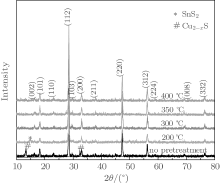
Figure 1 shows the XRD patterns of sulfurized CZTS films with pretreatment at indicated temperatures both without pretreatment and after sulfurization at 500 ° C for 2 h. According to the results, all of the samples have the same diffraction peaks at 2θ = 18.2° , 28.5° , 32.9° , 47.3° , 56.8° attributable to the kesterite CZTS (101), (112), (200), (220), and (312) (JCPDS No. 26-0575). But the sample P200 has an impurity peak at 14.8° , which indicates the presence of SnS2.[16] And according to the XRD result, the sample P0 has some Cu2− xS impurity. All of the samples including the un-pretreated one show (112) preference orientation. With the increase of the pretreatment temperature, the full width at half maximum (FWHM) of the (112) peak increases first, and then decreases. When the pretreatment temperature is 350 ° C, the FWHM of the sample is the smallest. So, we believe that the crystalline of P350 is the best among all of the samples.
 | Fig. 1. XRD patterns of CZTS films without pretreatment and pretreated at different temperatures. |
Due to the similar diffraction patterns of CZTS with those of Cu2SnS3 and ZnS, the XRD results cannot completely prove that the as-obtained thin films are CZTS. The phase structure of the as-prepared films P0, P200, P300, P350, and P400 was further investigated by Raman spectroscopy, as shown in Fig. 2. All of the samples present a main peak at 338 cm− 1, with two other smaller ones at 288 cm− 1 and 372 cm− 1, which are all CZTS Raman peaks.[17] The sample P200 also shows a characteristic peak of SnS2 at 314 cm− 1, [17] which is consistent with the XRD results. The FWHMs of P200, P300, P350, and P400 are all smaller than that of P0. Among the four pretreated samples, P350 has a relatively small FWHM. Therefore, we speculate that P350 has the best crystallization in all of the samples.
 | Fig. 2. Raman spectra of CZTS films without pretreatment and pretreated at different temperatures. |
Figure 3 shows the surface SEM images of the CZT precursors pretreated at different temperatures. From the images, we can see that grains at the surfaces of the as-prepared thin films grow large with increasing pretreatment temperature. The melting points of Sn, Zn, and Cu are 231.89 ° C, 491.5 ° C, and 1083.4 ° C, respectively. When the pretreatment temperature is 200 ° C, it is lower than the melting points of the metals. So, the surface morphology is basically unchanged. However, when the precursors are pretreated at 300 ° C, Sn melts and diffuses into Cu and Zn, which promotes to form large grains, as shown in Fig. 3(c). Figure 4 demonstrates the SEM images of CZTS prepared with different pretreatment temperatures and after sulfurization at 500 ° C for 2 h. According to Fig. 4, the grain sizes of P200, P300, P350, and P400 are larger than that of P0. P350 has a compact surface with homogenous grain size. Holes are found on the surface of sample P400 in the figure. The results indicate that the pretreatment is good for the growth of grain in a limited temperature range. Figure 4(f) shows the cross-sectional SEM image of the CZTS thin film pretreated at 350 ° C and after sulfurization. The cross-sectional image indicates a homogeneous and dense morphology without any voids at the substrate/CZTS interface. The thickness of the as-prepared CZTS thin film is about 1.38 μ m.
There is difficulty in controlling the ratio of the four elements in the preparation of the CZTS thin film. In the two-step method, Sn is easy to volatilize during the sulfurization process. Gurav et al.[18] reported that after being pretreated at different temperatures, the electrodeposited metal stacks showed Cu6Sn5 and Cu5Zn8 alloy phases, which were formed gradually with increasing pretreatment temperature. Thus, the pretreatment is effective for forming alloys between metal films first, which could weaken the problem. The EDS results of the as-prepared CZTS films are showed in Table 1. All of the Sn contents in the pretreated samples are much higher than that in the untreated one, among which the Cu: Zn: Sn: S ratio
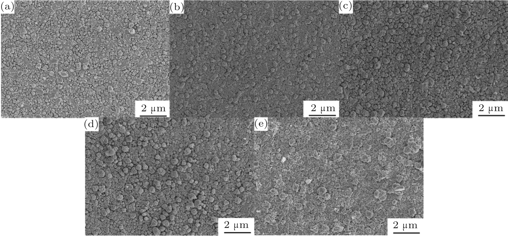 | Fig. 3. SEM images of CZT metal precursors pretreated at different temperatures: (a) no pretreatment, (b) 200 ° C, (c) 300 ° C, (d) 350 ° C, (e) 400 ° C. |
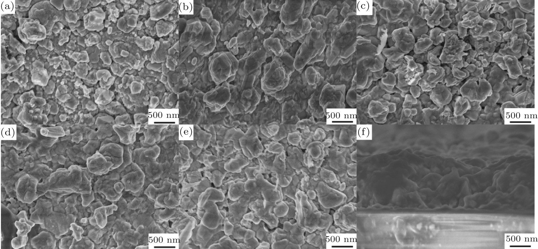 | Fig. 4. SEM images of CZTS films prepared with different pretreatment temperatures: (a) no pretreatment, (b) 200 ° C, (c) 300 ° C, (d) 350 ° C, (e) 400 ° C; (f) cross-sectional image of CZTS film pretreated at 350 ° C. |
of P350 is the closest to 2 : 1 : 1 : 4. The results show that the pretreatment can effectively reduce the Sn volatilization. The sequence and the thicknesses of the metallic films, as well as the sulfurization pressure, have a great influence on the properties of the CZTS thin films.[19] For example, due to the Sn volatilization, the CZTS films have very rough surfaces and bad adhesion.[20] The pretreatment in this work could solve this problem. More optimizations are needed to get even improved CZTS films for the solar cell application.
Figure 5 shows the reflectance and transmittance spectra of the CZTS films pretreated at different temperatures. As we can see, P0 has the highest reflectance and transmittance. After the pretreatment, the reflectance and transmittance of all the samples obviously decrease. Particularly, in the visible light region of 400– 800 nm, P350 has a low reflectance, which is lower than 10%. Moreover, the transmittance of the sample in the same region is nearly 0%. When the wavelength is longer than 800 nm, the transmittance of P350 increases dramatically.
| Table 1. The EDS results of CZTS films without pretreatment and pretreated at different temperatures. |
 | Fig. 5. (a) Reflectance and (b) transmittance spectra of CZTS films pretreated at different temperatures. |
By combining the reflectance and transmittance results, the optical absorption coefficient is calculated. As shown in Fig. 6, the optical absorption coefficients of all of the samples are much larger than 104 cm− 1 in the visible region. Especially in the wavelength of 400– 500 nm, the value reaches near 105 cm− 1.
 | Fig. 6. (a) Absorption coefficients and (b) (α hν )2 versus photon energy of CZTS films pretreated at different temperatures. |
Since CZTS is a direct band gap semiconductor, the absorption coefficient has a relationship with band gap Eopt[21]

where Eopt is the band gap, and B is a constant. The band gap is obtained by extrapolating the linear portion of the curve to the x axis. As shown in Fig. 6(b), the band gap is 1.61 eV for P0, 1.63 eV for P200, 1.43 eV for P300, 1.49 eV for P350, and 1.45 eV for P400. The band gaps of P300, P350, and P400 are consistent with that of the bulk CZTS (1.4– 1.6 eV).[22, 23] Due to the secondary phases of Cu2− xS and SnS2, the band gaps of P0 and P200 are larger than 1.6 eV. Because the band gap of P350 is close to 1.5 eV, P350 may be suitable as the absorption layer of solar cells.
The effect of the pretreatment temperature of CZT precursors on the structural, compositional, and morphological properties of CZTS films was demonstrated. It was found that the characteristics of the CZTS film were strongly dependent on the pretreatment temperature of the CZT precursor. The XRD results showed that the samples with pretreatment at 350 ° C had the best crystallization. All of the FWHMs of the main Raman peaks from the pretreated samples were smaller than those of the untreated one, indicating that the pretreatment process could improve the crystallization of the CZTS film. The surface of the film was compact and the grain size was homogeneous under a lower pretreatment temperature, while holes started to appear when the temperature reached 400 ° C. The sample pretreated at 350 ° C demonstrated an optical absorption coefficient much higher than 104 cm− 1 in the visible region and a band gap of 1.49 eV, which is very optimal for solar cell applications.
| 1 |
|
| 2 |
|
| 3 |
|
| 4 |
|
| 5 |
|
| 6 |
|
| 7 |
|
| 8 |
|
| 9 |
|
| 10 |
|
| 11 |
|
| 12 |
|
| 13 |
|
| 14 |
|
| 15 |
|
| 16 |
|
| 17 |
|
| 18 |
|
| 19 |
|
| 20 |
|
| 21 |
|
| 22 |
|
| 23 |
|