Liu Yue, Zhu Hao-Nan, Pei Zi-Dong, Kong Yong-Fa, Xu Jing-Jun. Molecular dynamic simulations of surface morphology and pulsed laser deposition growth of lithium niobate thin films on silicon substrate* . Chinese Physics B, 2015, 24(5): 056802
Permissions
Molecular dynamic simulations of surface morphology and pulsed laser deposition growth of lithium niobate thin films on silicon substrate*
Liu Yuea), Zhu Hao-Nanb), Pei Zi-Donga), Kong Yong-Faa),c)†, Xu Jing-Juna)‡
The MOE Key Laboratory of Weak-Light Nonlinear Photonics and TEDA Applied Physics School, Nankai University, Tianjin 300457, China
School of Mathematical Science, Peking University, Beijing 100871, China
R & D Center, Taishan Sports Industry Group, Leling 253600, China
*Project supported by the National Basic Research Program of China (Grant No. 2011CB922003), the International S&T Cooperation Program of China (Grant No. 2013DFG52660), the Taishan Scholar Construction Project Special Fund, China, and the Fundamental Research Funds for the Central Universities, China (Grant Nos. 65030091 and 65010961).
Abstract
The molecular dynamic simulation of lithium niobate thin films deposited on silicon substrate is carried out by using the dissipative particle dynamics method. The simulation results show that the Si (111) surface is more suitable for the growth of smooth LiNbO3 thin films compared to the Si(100) surface, and the optimal deposition temperature is around 873 K, which is consistent with the atomic force microscope results. In addition, the calculation molecular number is increased to take the electron spins and other molecular details into account.
Lithium niobate (LiNbO3, or LN) has been intensively studied due to its interesting electro-optic, acousto-optic, elasto-optic, piezoelectric, pyroelectric, and nonlinear optical properties. Moreover, it can be easily doped with laser-active ions, which allows the simple fabrication of low-loss optical waveguides. In industry, LiNbO3 has been considered as the “ silicon of nonlinear optics” or “ silicon of photonics[1] due to its versatility. Because silicon is the backbone of integrated electronics, [2] growing a LiNbO3 thin film on silicon would be helpful to integrate optic and electric devices on one chip.
Several methods have been reported to fabricate LiNbO3 thin films on silicon, such as molecular beam epitaxy (MBE), pulsed laser deposition (PLD), and liquid phase epitaxy (LPE).[3, 4] Since the crystal structure of LiNbO3 is a distorted perovskite, and the lattice parameters are a = b = 5.15 Å , c = 13.863 Å , while silicon belongs to the diamond type, and the lattice parameter is a = 5.431 Å . The lattice mismatch, which is 5.2%, makes it difficult to grow high quality LiNbO3 thin films on the Si substrate. In experiment, the LiNbO3 film quality is sensitive to many parameters, such as temperature, substrate orientation, substrate morphology, target, and chamber atmosphere.[5– 7] So far, the ideal growth conditions of high quality LiNbO3 crystal are still under debate.
Recently, several methods have been used to simulate thin film growth, [8] such as the molecule dynamics, Monte Carlo, and kinetic Monte Carlo methods.[9– 12] These simulations have revealed the microscopic dynamics and the influence of the temperature on assembling particles. However, the calculation is slow and the time scale is short with limited particles considered.
The dissipative particle dynamics (DPD) method was developed by Koelman and Hoogerbrugge, [13, 14] which allows longer-time scale calculation and larger system simulation.[18] The DPD method has been used in studying a surfactant among water moleculars.[15, 16] Ryjkina et al.[15] and Kuo et al.[16] reported that the DPD method can also be used in liquid molecular aggregation.
In the PLD thin film growth process, the relative positions and velocities of the particles satisfy the proper conservation laws and symmetries, and the momentum transferred from the particles also satisfies the linear and angular conservations, which meet the demands of the DPD method. In this work, we apply the DPD method to the solid molecular field, which shows that the PLD process can be reproduced by the DPD technique. As a result, we find the optimal deposition temperature and substrate.
2. Simulation method and experiment
The lithium niobate molecule and the silicon atom are chosen to be the DPD particles to understand the lithium niobate morphology on the silicon substrate. Assume that the lithium niobate molecules are in stoichiometry (Li-Nb-O3) and electric neutrality under ideal target and oxygen atmosphere, and the total number is 1 × 10⁶ in one simulation. The LiNbO3 molecular lattice parameters are a = b = 0.515 nm, c = 1.3863 nm, and the average parameter is ā = (a + b + c)/3 = 0.808 nm. In the two-dimensional simulation of a 100 nm × 100 nm film, the average thickness of the simulated film is h = 0.808 × 10⁶/100/100 = 80.8 nm. Consider the ideal condition which does not include the defects and supposes that the particles at the boundaries are in balance. The thickness is at the same level with the atomic force microscope (AFM) results and the previous results (50 nm).[13] Approximately, the whole progress in PLD is designed to deposit on the silicon surface of 100 nm × 100 nm at different temperatures. The unreconstructed Si(111) and Si(100) surfaces are selected as the deposition surface.
The final position of a DPD particle is determined by the force exerted on it. The time evolution of the process follows Newton’ s law. A DPD particle is affected by the neighbor DPD particles via three non-bonded forces: a conservative force FC, a dissipative force FD, and a random force FR. Therefore, the effective force Fi acting on particle i is given by[14]
where i, j represent the DPD particles of the lithium niobate molecule and silicon atom, respectively. The FC is a repulsive central force with a maximum value aij as shown in Ref. [15]
where aij, eij, rij, rc are the maximum repulsive parameter, the unit vector, the distance between particles i and j, and the cutoff radius, respectively.
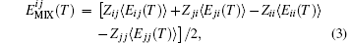
To calculate FC, aij must be calculated. Here the interaction parameter is obtained by considering the mean pair contact interaction energy ⟨ Eij(T)⟩ between lithium niobate molecules and silicon atoms. First, we calculate the mixing energy between two DPD particles i and j according to[16]
where Z′ s are the coordination numbers of each DPD particle pair. The averaged pair interaction energy ⟨ E(T)⟩ is optimized. The electron state is set as the ground state, with default spin and B3LYP based on the density function theory (DFT) using Gaussian software. The basis set is 6-31G and no charge. Therefore, the electron spin is considered and the energy between particles i and j is optimized. These calculated averaged mixing energies are used to obtain the Flory– Huggins interaction parameter χ ij(T), [17]
The χ parameter is used to determine the maximum repulsive force aij between particles i and j, [17]
where the terms are affected by the interaction between the pure DPD particles i (aii = 15kBT).[18] The force and are responsible for the conservation of the total momentum in the system. To calculate and , the parameters are derived from Groot and Warren.[19] The whole programming is realized in Mathematica.
The LiNbO3 thin films are grown on Si(111) and Si(100) at 873 K for 2 h, and in-situ annealed for 1 h by the PLD. The target is LiNbO3 single crystal, the gas pressure is 30 Pa, the excimer laser wavelength is 248 nm, and the pulse width is 25 ns. The thin films’ morphology is investigated by atomic force microscopy (AFM) at room temperature.
3. Results and discussion
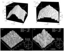
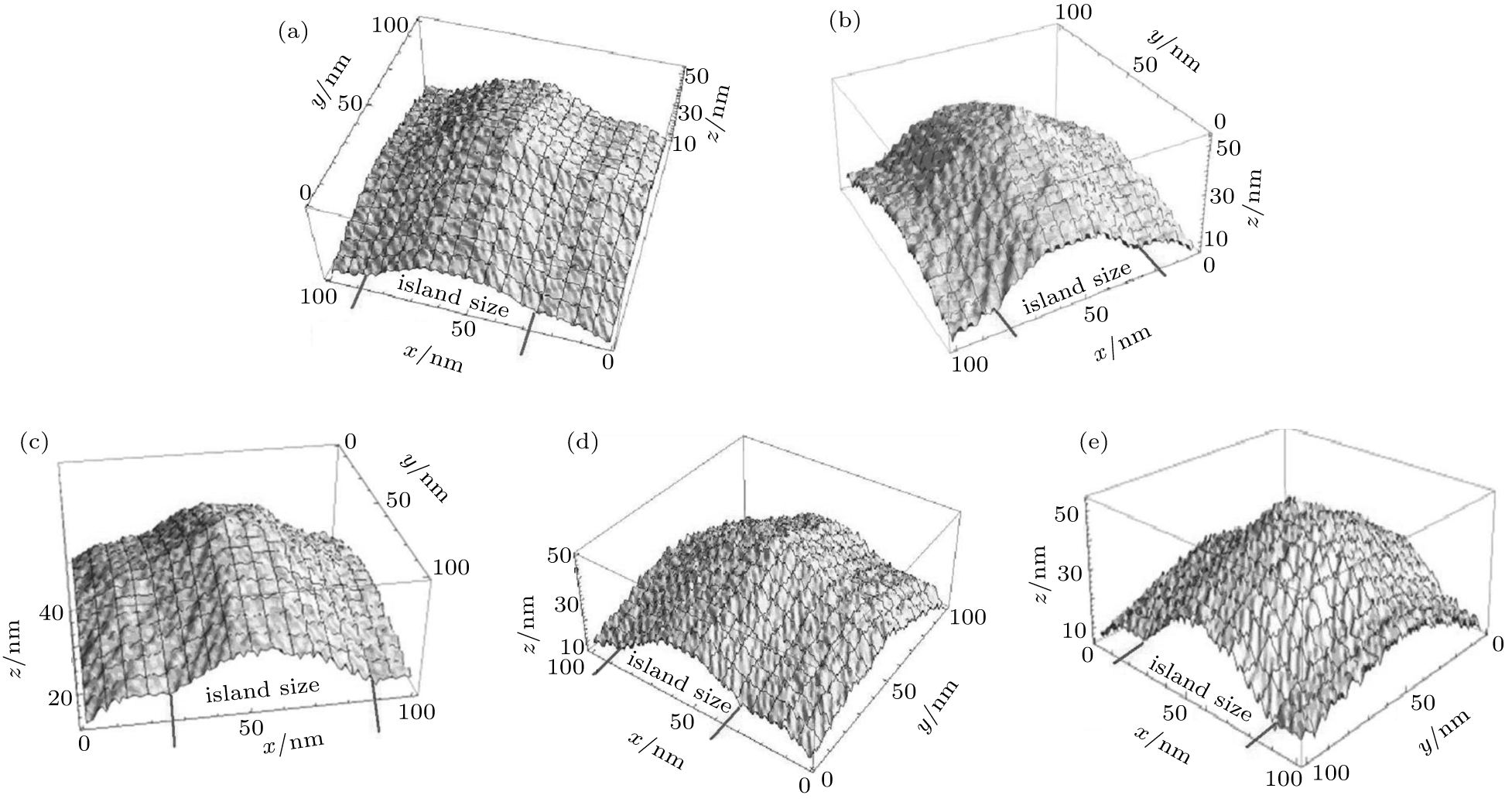
The deposition on Si(111) and Si(100) substrates at five different temperatures (723 K, 773 K, 823 K, 873 K, and 923 K) is simulated. Figure 1 shows the simulated and experimental results of lithium niobate deposited on different silicon surfaces at 873 K. Figures 1(a) and 1(c) are both on the Si(111) surface, and figures 1(b) and 1(d) are on Si (100). The simulations and experiments are consistent with each other on the island sizes and heights. As labeled by the red lines, the island edge is chosen to be the lowest line of the simulation picture and AFM results. Based on this, the growth conditions can be optimized to obtain a smooth surface. In the DPD simulation, the Si(111) surface leads to smaller island size of 55– 65 nm, which is similar with the AFM results (40– 90 nm) in Fig. 1(c). On the Si(100) surface, the edges of the simulated LiNbO3 islands cannot be observed, suggesting that the simulated LiNbO3 island is larger than 100 nm on average, as shown in Fig. 1(b), which is consistent with the AFM image in Fig. 1(d). The island heights are almost the same (∼ 50 nm) on Si(111) and Si(100), both experimentally and theoretically. The results show that LiNbO3, in terms of morphology, is more suitable to be deposited on the Si(111) surface compared with the Si(100) one.
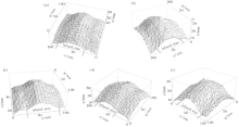
The simulation results are meaningful, which indicate that the DPD method is feasible to simulate the thin film growth of complex oxides. The simulation results of LiNbO3 thin films grown on Si(111) substrate at different temperatures are shown in Fig. 2. The smallest island size is found to be optimized (55 nm) at 873 K, while most are between 60 nm and 64 nm at other temperatures. At 873 K, the film can becomes smoother because lower temperatures concentrate LiNbO3 molecules on silicon and higher temperatures reduce the repulsive force in Eq. (4). Moreover, 873 K was reported as the proper temperature to grow smooth LiNbO3 thin films on Si(111).[7] For the morphology, the simulation result of 873 K is consistent with the reference.
Fig. 1. (a), (b) DPD simulation results for lithium niobate deposited on different silicon surfaces at 873 K; (c), (d) AFM images of LiNbO3 thin films deposited on silicon substrates by LMBE at 873 K: (a) and (c) on Si(111); (b) and (d) on Si(100).
Fig. 2. The DPD simulation results for lithium niobate deposited on Si(111) surface at different temperatures: (a) 673 K, (b) 723 K, (c) 773 K, (d) 873 K, (e) 923 K.
4. Summary
The DPD simulation suggests that the Si(111) surface is more suitable to produce smooth LiNbO3 thin films than the Si(100) surface. In addition, the optimal deposition temperature is found to be around 873 K, which is consistent with the experimental results. The results indicate that the DPD method is reliable for the simulation of thin film growth of complex oxides, which provides a new path for calculating the defects and the speed distribution of particles.
... silicon of photonics[1] due to its versatility ...
1
1998
0.0
0.0
... Because silicon is the backbone of integrated electronics,[2] growing a LiNbO3 thin film on silicon would be helpful to integrate optic and electric devices on one chip ...
1
2006
14.829
0.0
... [3,4] Since the crystal structure of LiNbO3 is a distorted perovskite, and the lattice parameters are a #cod#x003D ...
1
1990
0.71
0.0
... [3,4] Since the crystal structure of LiNbO3 is a distorted perovskite, and the lattice parameters are a #cod#x003D ...
1
1995
3.794
0.0
... [5#cod#x02013 ...
1
2001
1.545
0.0
2
2007
1.534
0.0
... 7] So far, the ideal growth conditions of high quality LiNbO3 crystal are still under debate ...
... [7] For the morphology, the simulation result of 873#cod#x00A0 ...
1
2012
0.0
0.0
... Recently, several methods have been used to simulate thin film growth,[8] such as the molecule dynamics, Monte Carlo, and kinetic Monte Carlo methods ...
1
1998
7.943
0.0
... [9#cod#x02013 ...
1
2010
3.794
0.0
1
1995
0.0
0.0
1
2010
3.794
0.0
... 12] These simulations have revealed the microscopic dynamics and the influence of the temperature on assembling particles ...
2
2003
0.0
0.0
... The dissipative particle dynamics (DPD) method was developed by Koelman and Hoogerbrugge,[13,14] which allows longer-time scale calculation and larger system simulation ...
... [13] Approximately, the whole progress in PLD is designed to deposit on the silicon surface of 100#cod#x00A0 ...
2
1992
2.26
0.0
... The dissipative particle dynamics (DPD) method was developed by Koelman and Hoogerbrugge,[13,14] which allows longer-time scale calculation and larger system simulation ...
... Therefore, the effective force Fi acting on particle i is given by[14] ...
3
1993
2.26
0.0
... [15,16] Ryjkina et al ...
... [15] and Kuo et al ...
... [15] ...
3
2002
0.0
0.0
... [15,16] Ryjkina et al ...
... [16] reported that the DPD method can also be used in liquid molecular aggregation ...
... First, we calculate the mixing energy between two DPD particles i and j according to[16] ...
2
2004
3.349
0.0
... ij(T),[17] ...
... parameter is used to determine the maximum repulsive force aij between particles i and j,[17] ...
2
1995
2.26
0.0
... [18] The DPD method has been used in studying a surfactant among water moleculars ...
... [18] The force and are responsible for the conservation of the total momentum in the system ...
1
1997
1.578
0.0
... [19] The whole programming is realized in Mathematica ...


 , Xu Jing-Jun