

Influence of heavy ion irradiation on DC and gate-lag performance of AlGaN/GaN HEMTs*
[Lei Zhi-Fenga), b) , Guo Hong-Xiac)†  , Zeng Chang
a) , Chen Huia) , Wang Yuan-Shenga) , Zhang Zhan-Ganga) ]
, Zeng Chang|
|


†Corresponding author. E-mail: leizf@ceprei.com
*Project supported by the National Natural Science Foundation of China (Grant No. 61204112).
AlGaN/GaN high electron mobility transistors (HEMTs) were irradiated by 256 MeV127I ions with a fluence up to 1×10¹⁰ ions/cm2 at the HI-13 heavy ion accelerator of the China Institute of Atomic Energy. Both the drain current Id and the gate current Ig increased in off-state during irradiation. Post-irradiation measurement results show that the device output, transfer, and gate characteristics changed significantly. The saturation drain current, reverse gate leakage current, and the gate-lag all increased dramatically. By photo emission microscopy, electroluminescence hot spots were found in the gate area. All of the parameters were retested after one day and after one week, and no obvious annealing effect was observed under a temperature of 300 K. Further analysis demonstrates that swift heavy ions produced latent tracks along the ion trajectories through the hetero-junction. Radiation-induced defects in the latent tracks decreased the charges in the two-dimensional electron gas and reduced the carrier mobility, degrading device performance.
Researchers have demonstrated remarkable advances in microwave and low noise operation of AlGaN/GaN high electron mobility transistors (HEMTs) over the past few years.[1– 3] Potential applications for such devices include broad-band satellite transmission for communications, television, weather forecasting systems, nuclear reactors, and military systems.[4] Space applications require radiation resistance, so the mechanisms of radiation-induced degeneration should be studied. It is expected that GaN-based electronic devices will be considerably more radiation-resistant than their more conventional GaAs-based counterparts due to the higher displacement energy of the nitride materials. However, many research results show that ion-irradiation can make GaN HEMTs degenerate. High concentrations of the two-dimensional electron gas (2DEG) produced as a result of the material polarization of the AlGaN/GaN hetero-junction interface is the basis of AlGaN/GaN HEMTs, so the materials, structures, carrier generation, and transport mechanisms are apparently different from other semiconductor devices. The mode and mechanisms of AlGaN/GaN HEMTs’ degradation caused by radiation are very complex.
The radiation environment of outer space can be divided into three categories.[5, 6] The first is trapped particle environment, which comprises two regions called the inner and outer Van Allen belts for electrons, protons, and heavy ions. The second are the decay products of the cosmic ray environment, which comprises 85% protons, 14% α -particles, and 1% of heavier ions with an atomic number up to 92. The most abundant elements are carbon, oxygen, and iron nuclei. The third is the solar flare particle environment, which comprises protons, electrons, α -particles, and heavy ions. Altogether, the energy and flux ranges of interest include up to 100 MeV and 107– 109 particles· cm− 2/day for the protons and up to 10 GeV and 105– 107 particles· cm− 2/day for heavy ions. A satellite located at any near-earth orbit will be exposed to a flux of high energy particles from any of the above mentioned environments. Recently, GaN-based devices have been studied by subjecting them to protons, neutrons, and low energy heavy ion irradiation, and the DC performance was degraded somewhat after irradiation, [7– 10] but few researchers have tested the gate-lag and electroluminescence after heavy ion irradiation. In the present work, we have tested, for the first time, both gate-lag performance and electroluminescence distribution after exposure to heavy-ion irradiation of 265 MeV 127I ions with a fluence of 1 × 10¹⁰ ions/cm2.
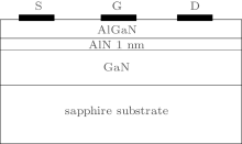
Figure 1 is a schematic of the AlGaN/GaN HEMTs used for this work. The DUT was fabricated starting from epitaxial structures that consist of a 2-nm GaN cap layer, a 18-nm AlGaN barrier layer, a 1-nm AlN spacer layer, a 2-μ m GaN buffer layer, and a GaN transition layer grown on SiC substrate. A sandwich of Mo/Pt/Au (30/40/300 nm) metals was evaporated to form Schottky gate contacts and another sandwich of Ti/Al/Ni/Au (20/30/50/100 nm) metals was used for the source and drain ohmic contacts. The devices have a gate length of 0.5 μ m, a gate width of 1.5 mm, and gate– source and gate– drain spacing of 2 μ m and 5 μ m, respectively.
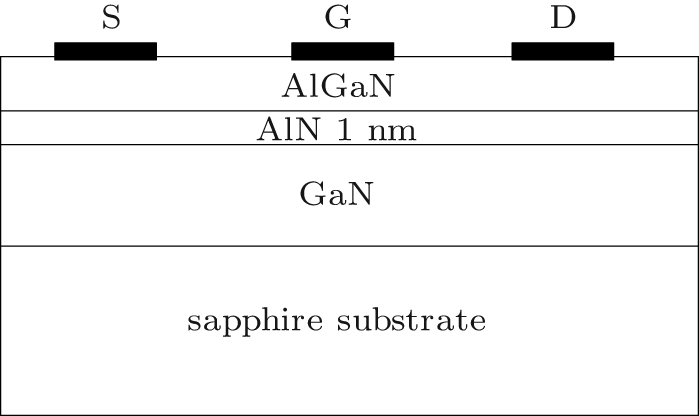 | Fig. 1. Schematic diagram of the details of AlGaN/AlN/GaN HEMT structures (not to scale). |
Iodine ions at 265 MeV were chosen for our irradiation experiment at the HI-13 heavy ion accelerator of China Institute of Atomic Energy. The beam flux was about 106 ions/(cm2· s) with a total fluence of up to 1 × 10¹⁰ ions/cm2. By Monte Carlo simulation in SRIM 2003 (Stopping and Range of Ions in Matter), the electronic and nuclear stopping powers of 265 MeV 127I ions in GaN are found to be 29.92 keV/nm and 0.081 keV /nm, respectively, and the projected ion range is 12.5 μ m. Hence, those ions lose their energy predominantly in the electronic stopping power regime throughout the entire 2-μ m-thick GaN film, while the ion end-of-range region is deep inside the sapphire substrate. All of the ions were at normal incidence, and all of the tests were performed under room temperature.
During irradiation, the drain-source voltage (VDS) was 20 V, and gate– source voltage (VGS) was − 3 V. Before and after irradiation, the electrical parameters were all measured under room temperature, including DC output, transfer characteristics, gate leakage and gate-lag performances by B1500A semiconductor parameter analyzer. The device was also characterized by photo emission microscopy (PEM). About two days and again at one week after the irradiation, the same measurements were performed to confirm the existence of an annealing effect.
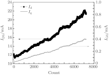
In the irradiation test, the drain-source and the gate current were monitored in off-state with bias of VGS − 3 V and VDS 20 V, and the results are shown in Fig. 2. It is obvious that both the drain current Id and the gate current Ig increased during heavy ion irradiation.
 | Fig. 2. The drain-source and gate current monitored results under irradiation. |
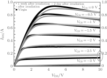
Figure 3 shows the drain-source current as a function of drain-source voltage (IDS– VDS) characteristics before and after heavy ion irradiation. The gate voltages are 0 V, − 0.5 V, − 1 V, − 1.5 V, − 2 V, − 2.5 V, and − 3 V, respectively. It can be seen from Fig. 1 that after irradiation, the saturation current IDS increases. In the case of gate voltage of − 2.5 V and drain-source voltage of 10 V, the IDS increases by almost 40% after irradiation, from 135 mA to 190 mA. Moreover, there is also a decrease in the initial slope of the current curve at low bias, which indicates a change in carrier mobility or density. The output characteristics were measured again about one week after irradiation and the results were the same. This means that there are no annealing effects under room temperature.
 | Fig. 3. Output characteristic curves of the HEMT device before and after irradiation. |
The transfer characteristics of DUT were tested with a drain-source voltage of 2 V before and after the heavy ion irradiation. The results are shown in Fig. 4. It can be seen that the threshold voltage after irradiation decreases by about 4.7%, from − 2.78 V to − 2.91 V. Moreover, the maximum trans-conductance decreased by about 13%. The transfer characteristics after one week were the same as that after irradiation, so there are also no annealing effects in the transfer characteristics at room temperature.
 | Fig. 4. Transfer characteristic curves of the HEMT device before and after irradiation. |
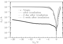
Figure 5 shows the gate characteristics of the HEMT before and after heavy ion irradiation. The gate leakage current after irradiation was significantly increased with a fluence of 1 × 10¹⁰ ions/cm2. At the negative gate voltage of − 10 V, the gate leakage current increased from 0.6 μ A to 1 mA, more than three orders of magnitude from the value before irradiation.
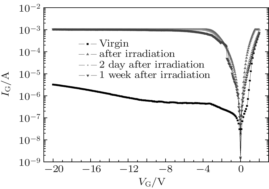 | Fig. 5. Gate leakage curves of the HEMT device before and after irradiation. |
Usually, the mechanisms of gate leakage involve surface generation recombination in the low bias voltage region and an increase in channel resistance at a higher voltage.[11]
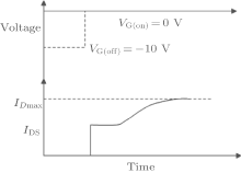
Gate lag can significantly limit the RF performance and long term reliability of GaN HEMTs.[12] Figure 6 schematically illustrates the gate lag. When the VGS is 0 V, the device is “ on” and the drain current is at its maximum value. When VGS is − 10 V, the device is off. However, when VGS changes to 0 V, the drain current does not immediately return to the peak current level, this is the gate lag. Gate lag can significantly limit RF performance and the long-term reliability of AlGaN/GaN HEMTs, so its effects are important in order to characterize GaN response in a space environment.
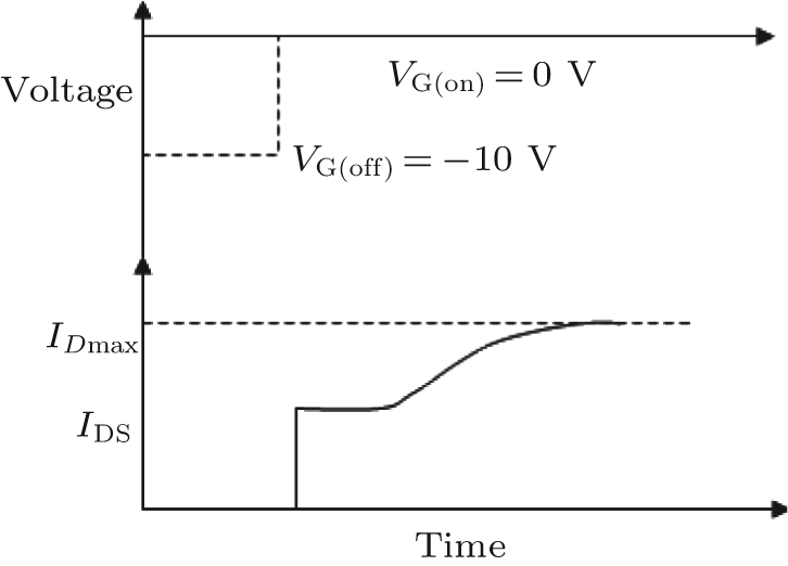 | Fig. 6. Schematic of gate lag in AlGaN/GaN HEMTs. |
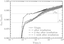
Figure 7 shows the gate-lag characteristic before and after irradiation. The current collapse before irradiation was about 1%, but after irradiation it increased to 2%. The gate lag in un-irradiated GaN devices has been attributed to two mechanisms, trapping in the bulk GaN region of the device and trapping on the AlGaN surface.[13, 14] The gate lag due to surface traps originates from temporary variations in the occupancy of donor traps in the access regions next to the gate (source-gate, drain-gate). The gate lag due to bulk traps in the GaN buffer region may also occur, due to the trapping of hot electrons generated in the 2DEG under the gate edges. This depletes the 2DEG and causes a reduction in the drain current. The magnitude of the reduction in drain current depends on trap density and distribution, trap energy, and the presence or absence of a passivation layer on the surface.
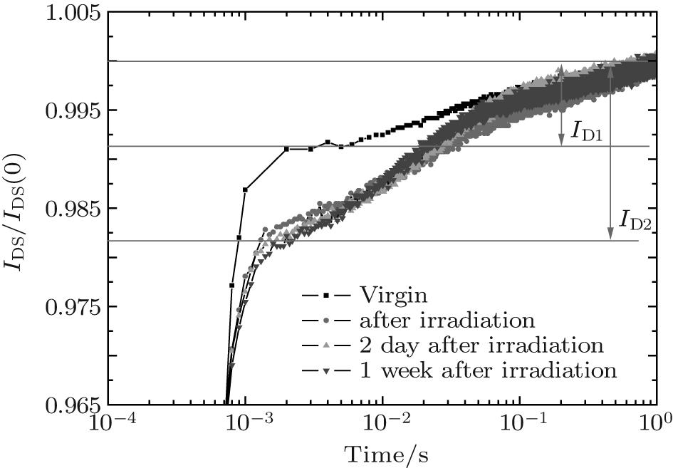 | Fig. 7. Gate lag before and after irradiation. |
Photo emission microscopy (PEM) was used to characterize the spatial distribution of electroluminescence (EL) to locate possible failure sites. The characterization of the intensity and spatial distribution of EL may have implications for detecting the structural damage in AlGaN/GaN HEMTs. As shown in Fig. 8, the spatial distribution of the EL intensity of the device after irradiation became non-uniform, with many hot spots appearing in the gate area. “ Hot spots” mean areas where leakage is more evident, and it is probable that high-energy heavy ions induce latent tracks as newly added leakage passages degrade the gate.
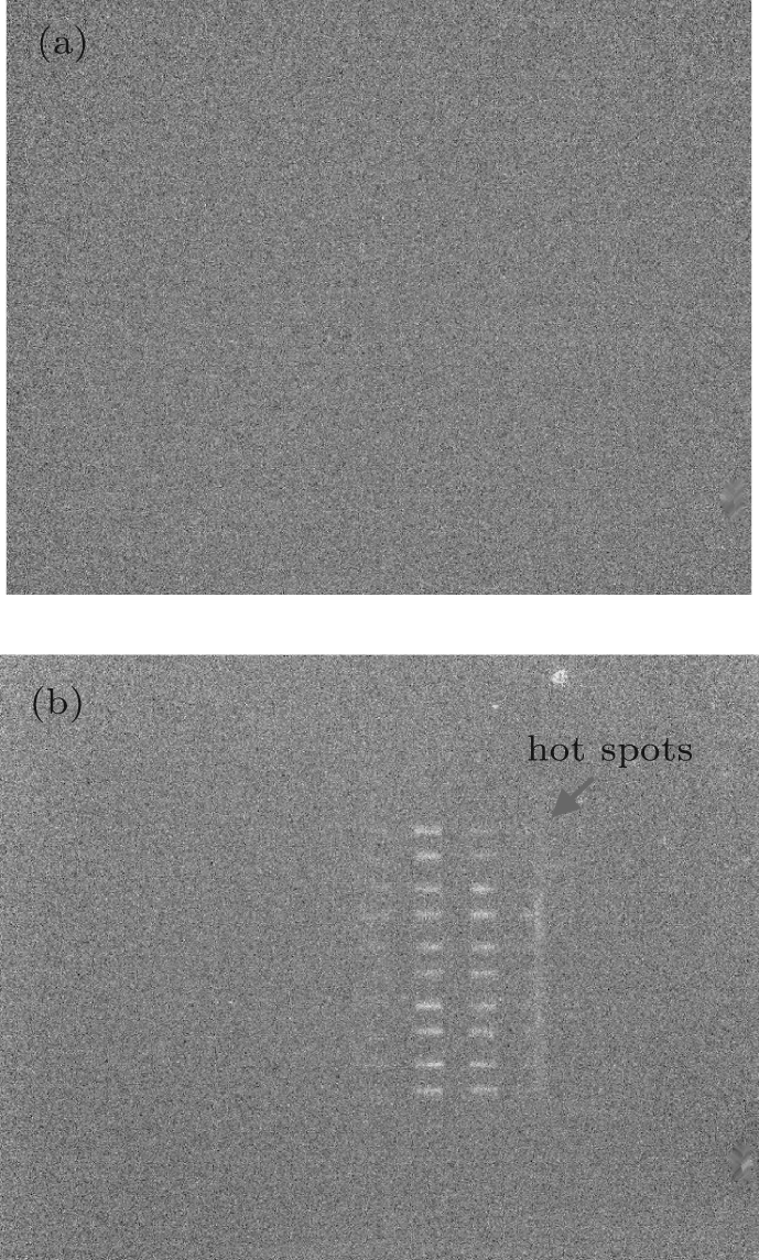 | Fig. 8. Spatial distributions of the EL intensity of the device in off-state (Vgs = − 10 V, 50× objective) (a) before and (b) after irradiation. |
For AlGaN/GaN HEMT devices, the current at position x in 2DEG channel is described as

where q is the electron charge, ns(x) is the concentration of 2DEG, w is the width of the gate, and v(x) is the velocity of the electron at x.
The value of v(x) changes with changing electric field intensity, and it is related to electron mobility. When the channel electric field is equal to or higher than the critical electric field Ec, the electrons reach saturation velocity vs, but when the voltage is lower than Ec, the electron velocity will be determined by mobility μ , that is,

so for the curve below the knee voltage in the output characteristics, the slope is expressed as I/E = qnsW μ , which means that the slope depends on the 2DEG density and mobility.
In the depletion approximation, the total charges of 2DEG are given by[15]

where d is the distance between the gate and the thin charge layer, VGS is the gate source voltage, ε (x) is the dielectric constant of AlGaN, EF is the Fermi level of the two-dimensional potential well, and x is the mole fraction of Al in AlGaN components.
The threshold voltage is given by
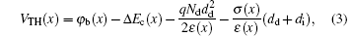
where Nd is the doping concentration in the AlGaN layer, dd is the thickness of the AlGaN layer, φ b(x) is the Schottky barrier height, Δ Ec(x) is the conduction band discontinuity, and di is the undoped AlGaN spacer layer thickness.
From Eqs. (1)– (3), we know that the saturation IDS depends on 2DEG concentration in the channel and on carrier mobility. The threshold gate voltage is influenced by doping density and the Schottky barrier height.
When ions impact semiconductor materials, they interact with the target atoms and extranuclear electrons, and electron– hole pairs are produced: this is an ionization effect. On the other hand, nuclear collisions result in displacement of the lattice atoms, and point defects are formed: if the nuclear energy loss is large enough, the secondary particles may further affect the lattice structure, and localized defect clusters are formed. It has been assumed in previous studies that lattice defects are produced as a result of nuclear collisions, while electronic energy loss processes have a negligible role in defect formation in GaN under bombardment with keV ions. Indeed for keV ions, low electronic energy losses of less than 1 keV/nm do not result in lattice defects in GaN.
However, for swift heavy ions (SHI) like 265 MeV 197I in this work, electronic energy loss can reach 29.92 keV/nm, inducing extremely intense electron– hole pairs. Then, ultra-fast excitation of valence electrons occurs along ion paths, which results in latent tracks in the DUT. This phenomenon was verified by Kucheyev’ work in GaN material using Au ions with energy of 200 MeV.[16] Such tracks are continuous or discontinuous cylindrical damaged zones created along the paths of rapidly moving ions. The hot spots of photo emission microscopy (PEM) test results illustrate many defects produced by 197I ion irradiation. The latent tracks produced by 265 MeV 197I ions would be new leakage paths, so the gate leakage of the post-irradiation device increased significantly. Meanwhile, radiation induced electron traps and trapped positive charges in the AlGaN layer act as trap-assisted-tunneling centers that also increase the gate leakage current.
The displacement effect in AlGaN / GaN HEMTs by heavy ions results in defects in the AlGaN barrier layer, as deep level trapping centers the defects distributed in the material randomly. At the same time, the ionization effect induces electron– hole pairs, the electrons will be swept out of the barrier layer because of its high mobility, and then the holes left will be trapped and form fixed positive charges. These fixed positive charges will make the conduction band more discontinuous. Then, the excited carrier intensity increases, and so the saturation of source-drain current increases and the threshold voltage negative drifts.
Aditya Kalavagunta’ s research showed that barrier layer surface traps are the primary cause of the gate lag.[12] Heavy ion bombardment results in more surface traps and increase the current collapse. In addition, heavy ion irradiation- induced traps in the barrier layer are fully filled when the gate voltage is − 10 V, but at the moment the gate voltage changes to 0 V, these trapped electrons need to be released immediately, which also results in an increase of the gate lag.
We investigated the influence of heavy ion irradiation on the electrical properties of AlGaN/GaN HEMTs. After irradiation by 256 MeV 127I ions with a fluence of 1× 10¹⁰ ions/cm2, an increase of drain current and a degradation of gate performance were observed, in which the saturation drain current increased about by 40% and the gate leakage current increased by approximately four orders of magnitude. The gate-lag transient electrical measurement technique was applied to analyze the degradation of the irradiated device. It was shown that the value of the drain current collapse increased to 2%, which is about two times the value before irradiation. Drain current, gate leakage, and gate lag of the irradiated device were measured after two weeks and no clear change was observed in those device characteristics, which indicates that there are no annealing effects in AlGaN/GaN HEMTs. Further analysis demonstrated that swift heavy ions produced latent tracks along the ion paths through the hetero-junction. These radiation-induced defects decreased the charges in the 2DEG and reduced the mobility, leading to the degradation of the device’ s performance. Radiation induced electron traps and trapped positive charges in the AlGaN layer act as trap-assisted-tunneling centers that increase the gate leakage current. Surface traps and bulk traps increase the amount of observed gate lag after irradiation.
This work was conducted at the HI-13 tandem accelerator located at the China Institute of Atomic Energy (CIAE). The authors are grateful for the support of the team, including Prof. Guo Gang, Dr. Shen Dong-Jun, Dr. Shi Shu-Ting, et al.
| 1 |
|
| 2 |
|
| 3 |
|
| 4 |
|
| 5 |
|
| 6 |
|
| 7 |
|
| 8 |
|
| 9 |
|
| 10 |
|
| 11 |
|
| 12 |
|
| 13 |
|
| 14 |
|
| 15 |
|
| 16 |
|