


Spectral enhancement of thermal radiation by laser fabricating grating structure on nickel surface*
[Liu Song, Liu Shi-Bing† ]
]
]
|
|


†Corresponding author. E-mail: sbliu@bjut.edu.cn
*Project supported by the National Natural Science Foundation of China (Grant No. 51275012).
Previous studies have shown some correlations between the optical properties of objects and their surface patterns. We fabricate tens of micrometer period gratings by femtosecond laser direct writing technology on polished nickel targets and measure their thermal radiation spectra at a temperature of 623 K by Fourier transform infrared (FTIR) spectrometry. The results show an obvious major enhanced peak in which the wavelength is slightly larger than the grating period. Surface plasmon resonance (SPR) and Kirchhoff’s law of thermal radiation are applied to give this phenomenon a preliminary explanation. In addition, we utilized rigorous coupled wave analysis (RCWA) to simulate the absorption spectrum of the grating surface. The experiment results show good agreement with the simulation results.
There is no doubt that every object emits thermal radiation from its surface when the temperature is greater than absolute zero. Wien gave the displacement law in 1893 that the peak wavelength of thermal radiation from a black body was in inverse proportion to its temperature. It reveals that one can identify the object’ s temperature by observing its surface color or measuring its thermal radiation spectrum, or deriving applications such as infrared temperature measurement, infrared radar, etc. With the rapid progress of science and technology, researchers find that when the surface pattern’ s characteristic length is compatible to the wavelength of light, novel phenomena will be shown. Ebbesen[1] observed the unusual zero-order transmission spectra on sub-wavelength hole array structures, and the surface plasmon resonance (SPR) enhanced effect is used to explain it. To enhance the light absorbtion or emission by nanostructures has become a popular research field[2, 3] in recent years. Thermal radiation, an electromagnetic wave in nature, can also be manipulated by the surface pattern through the SPR effect and gives potential prospective applications in infrared stealths, heating dissipation, etc. A systematical study of the regularity of selective thermal radiation enhancement with steel pattern depth and polarization was reported by Mason et al.[4, 5] Jiang et al.[6] showed a ten-fold enhancement of thermal radiation at a specific wavelength on the tri-layer with periodic home arrays plasmonic thermal emitters. Ueba et al.[7] used a split-ring resonator array to control the thermal radiation spectrally. Shimizu et al.[8] tried to use this technology to develop an advanced cooling system for electronic devices. Xuan[9] gave an overview on the micro/nano scale thermal radiation theory and applications. It shows that to manipulate thermal radiation spectrally is still a promising research field.[11– 14] Though lithography and electron beam etching technology can help to obtain precise and perfect micro/nano structure on the surface, it will take a fussy technical process and it is difficult to obtain large area structures when meeting industrial requirements.
Since femtosecond laser micro-structure processing becomes a promising method for fabricating desirable surface texture, researchers are able to get the structure which has a neat edge and almost no heat affected zone in a simple way, which suggests an easy way to spectrally manipulate thermal radiation and gives a prospect in infrared stealth applications. In this paper, we fabricate the one-dimesnional (1D) surface grating on nickel targets by femtosecond laser direct writing. An enhanced thermal radiation peak wavelength correlating with the grating period is observed. By virtue of the SPR and applying Kirchhoff’ s law of thermal radiation, a preliminary explanation for this phenomenon is performed. Computational results of the reflectance spectra in different grating periods through RCWA show good agreement with the experimental data.
Femtosecond laser direct writing is a simple and cheap way to fabricate structures in several microns, which especially shows proper feasibility in processing structures in a large area. For fabricating the grating structure, we used a Ti:sapphire laser system with a wavelength of 800 nm, the pulse duration at 35 fs and operating at a repetition rate of 1 kHz. The 10× objective with a 0.25 numerical aperture (NA) is used to focus the laser in order to get a tightly focused beam which makes the ablated area small. The nickel targets used in this experiment are cylinders with a diameter of 25 mm and a height of 10 mm, and the surface of the targets is polished to reduce the influence of surface roughness. A 3-axis motorized positioning system is used to translate the targets along the ‘ S’ path at a speed of 1 μ m/s. The resolution of this system is 0.017 μ m. In order to keep the duty ratio of grating at 0.5 and the depth of groove which is measured by an atomic force microscope and optical profiler around 1 μ m, we use an adjustable attenuation in front of the objective to control the laser pulse energy. The period of grating d is controlled at 5 μ m, 7 μ m, 10 μ m, 15 μ m, and 20 μ m by the high resolution motorized positioning system.
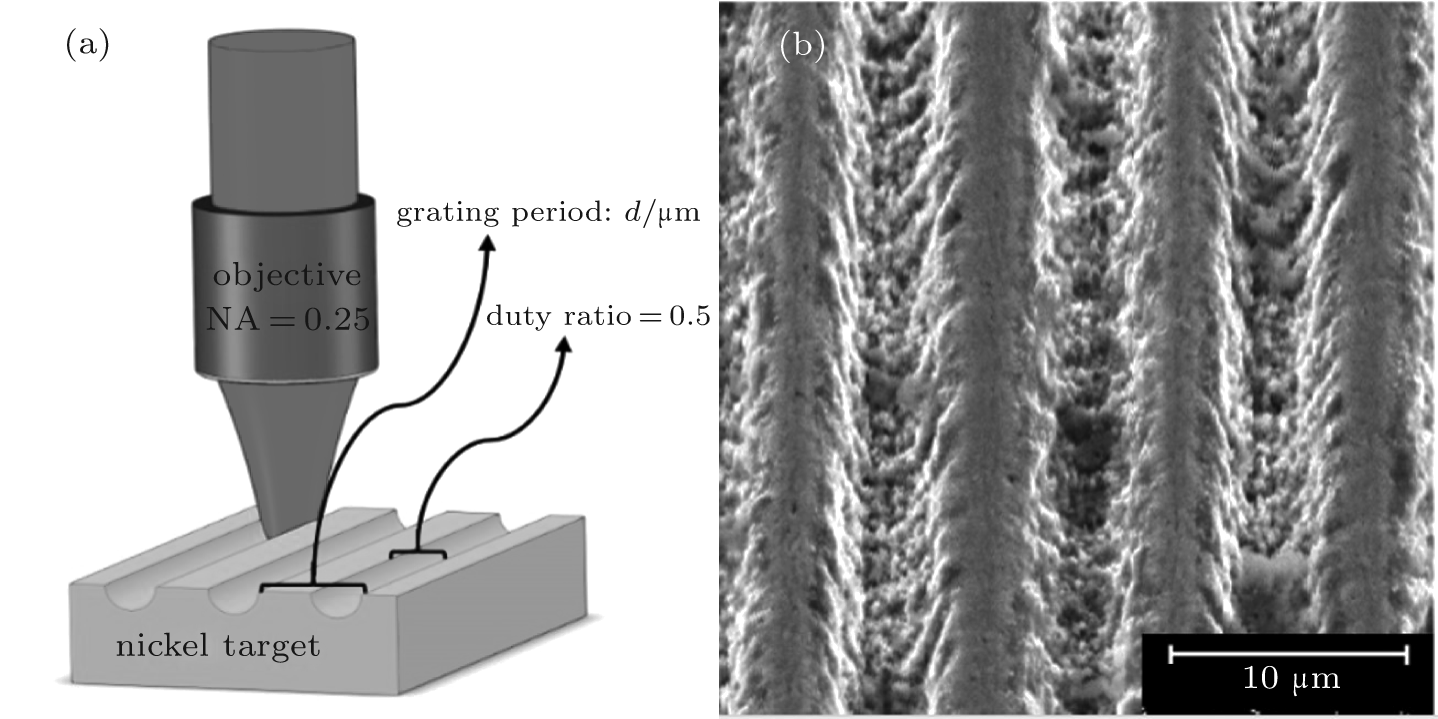 | Fig. 1. (a) The schematical diagram of laser processing nickel targets. The grating periods d of the surface are 5 μ m, 7 μ m, 10 μ m, 15 μ m, 20 μ m. (b) The surface topography of femtosecond laser fabricating grating measured by a scanning electron microscope. Though the fabricating quality of the femtosecond laser direct writing is not as good as lithography and electron beam etching, it has the advantage of being a simple technology and can be used in most materials. |
The thermal radiation spectra of fabricated nickel targets are measured by a Bruker Vertex 70 FTIR spectrometer. The infrared light emitted from the patterned surface of the nickel target which is heated by a temperature-controllable heater is collected by an off-axis parabolic mirror at a normal angle of 90° and passes through the external light source port of the FTIR spectrometer. The heated temperature is set to 623 K to obtain an appropriate intensity of thermal radiation to the spectrometer.
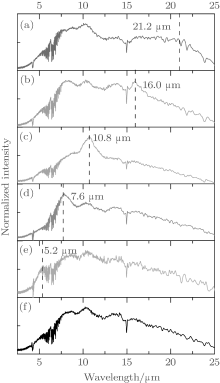
Figure 2 shows the infrared thermal radiation normalized spectra of the surfaces of nickel targets with different grating periods. Due to the response of the MCT (HgCdTe) detector and KBr beamsplitter limitations, the measurement range of the spectrum is 2.5 μ m and 25 μ m. From the spectra, we can learn that the thermal radiation energy is about 5 μ m– 20 μ m on a polished surface. It is obvious that the H2O and CO2 characteristic absorption peaks appear in the range of 4 μ m and 6 μ m− (− 8) μ m, respectively. For the grating surface with grating period d = 5 μ m, 7 μ m, 10 μ m, 15 μ m, and 20 μ m, the thermal radiation is enhanced at λ = 5.2 μ m, 7.6 μ m, 10.8 μ m, 16.0 μ m, and 21.2 μ m, respectively. The enhancement factors, calculated by dividing the original intensity of the grating surface by that of the polished surface at the wavelengths above, are 1.35, 1.80, 1.71, 1.54, and 1.84, respectively. It shows a substantial correlation between the enhanced thermal radiation wavelength and the surface grating period that the enhanced wavelength is slightly larger than the grating period.
 | Fig. 2. (a)– (e) The normalized thermal radiation spectra of grating surface with grating periods of 20 μ m, 15 μ m, 10 μ m, 7 μ m, and 5 μ m, respectively. (f) The normalized thermal radiation spectrum of the polished surface of nickel targets. |
It is widely convinced that the interpretation of this phenomenon is that SPR plays an important role in the interaction between the surface pattern and the electromagnetic wave.[5] The surface plasmon polariton (SPP) is an electromagnetic mode in the metal-dielectric interface due to the electron density oscillation. The wave vectors of photon kph and SPP kspp are given by


where ω is the frequency of light that excites the SPP, c is the light speed in a vacuum, θ is the normal angle of the incident light at the metal-dielectric interface, while ε m and ε d are the dielectric constants of metal and dielectric materials, respectively. As metal has a negative real part of the complex dielectric constant, at the same, ω the SPP wave vector kspp is always larger than the light’ s wave vector kph. It means that the light in a general sense cannot excite the SPP. After a number of theoretical derivations and experimental studies, researchers found that applying a surface grating structure will add an extra momentum kg to match the dispersion equation of light and SPP, giving a momentum match relation[10] as

where kg = 2π m/a and a is the period of grating, and m = ± 1, ± 2, … is the diffraction order. Since the nickel target is heated, thermal radiation emits from its surface and this electromagnetic wave excites the SPP with the assistance of surface grating. It causes a resonance at the wavelength which approximates to the grating period, resulting in the absorption enhancement at this wavelength. Because the thermal radiation is natural light and SPP is excited only for TM wave, the enhanced peak intensity as measured in Fig. 2 reduces to 1/2. According to Kirchhoff’ s law of thermal radiation, the objects’ emission is proportional to its absorption in thermodynamic equilibrium, hence the grating surface exciting the SPP leads to an obvious enhanced emission at the characteristic wavelength.
We utilize an open-source RCWA numerical simulating software to calculate the reflection spectrum of a 1D grating surface of nickel. The spectra of the grating periods of 5 μ m, 7 μ m, 10 μ m, 15 μ m, and 20 μ m are obtained by importing the dispersion value introduced by Ordal et al.[15] The results show that the reflectance reduces at the characteristic wavelengths of 5.8 μ m, 7.4 μ m, 10.2 μ m, 15.1 μ m and 20.1 μ m, respectively. Here, we consider that the slighter deviation of the characteristic wavelength between experiment and simulation results from the interaction of the uncurtained dispersion properties on the surface and the instability of laser fabricating. As the metal has a non-transmittance surface, the transmittance T equals 0, and absorptance equals (1 – R), where R is the reflectance. Figure 3 gives the absorptance spectra of different period gratings. It reveals that grating surface pattern has an absorption peak whose wavelength is near the grating period. By Kirchhoff’ s law of thermal radiation, we know that the thermal radiation is enhanced at these peaks.
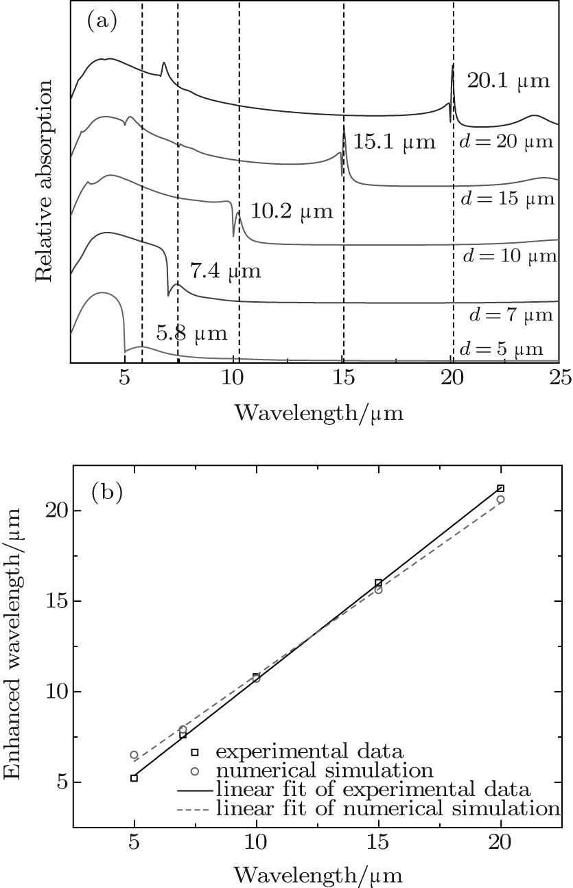 | Fig. 3. (a) The absorption spectra computed by RCWA. (b) Linear fitting of the experiment data shows good agreement with the results of numerical simulation. |
In addition, we calculate the relative intensity of the grating surface compared with the polished surface and the smooth spectral curve. In Fig. 4, we observe the half wavelength of major enhanced wavelength. On the grating surface with a grating period of 5 μ m, the enhanced wavelength is 5.2 μ m so that the half wavelength is theoretically 2.6 μ m which is in the low response area of the detector. Therefore there is no observation on the grating surface with a 5-μ m grating period. On the grating surface with a grating period of 7 μ m, there is a half wavelength of 3.9 μ m which is larger than half of 7.6 μ m. At grating periods of 10 μ m, 15 μ m, and 20 μ m, the observed half wavelengths are 5.3 μ m, 7.8 μ m, and 9.5 μ m, respectively, which are less than half of the corresponding major enhanced wavelengths. This phenomenon is commonly considered to be caused by the half of the resonant wavelength which is related to the diffraction order m = ± 2 in grating momentum kg.
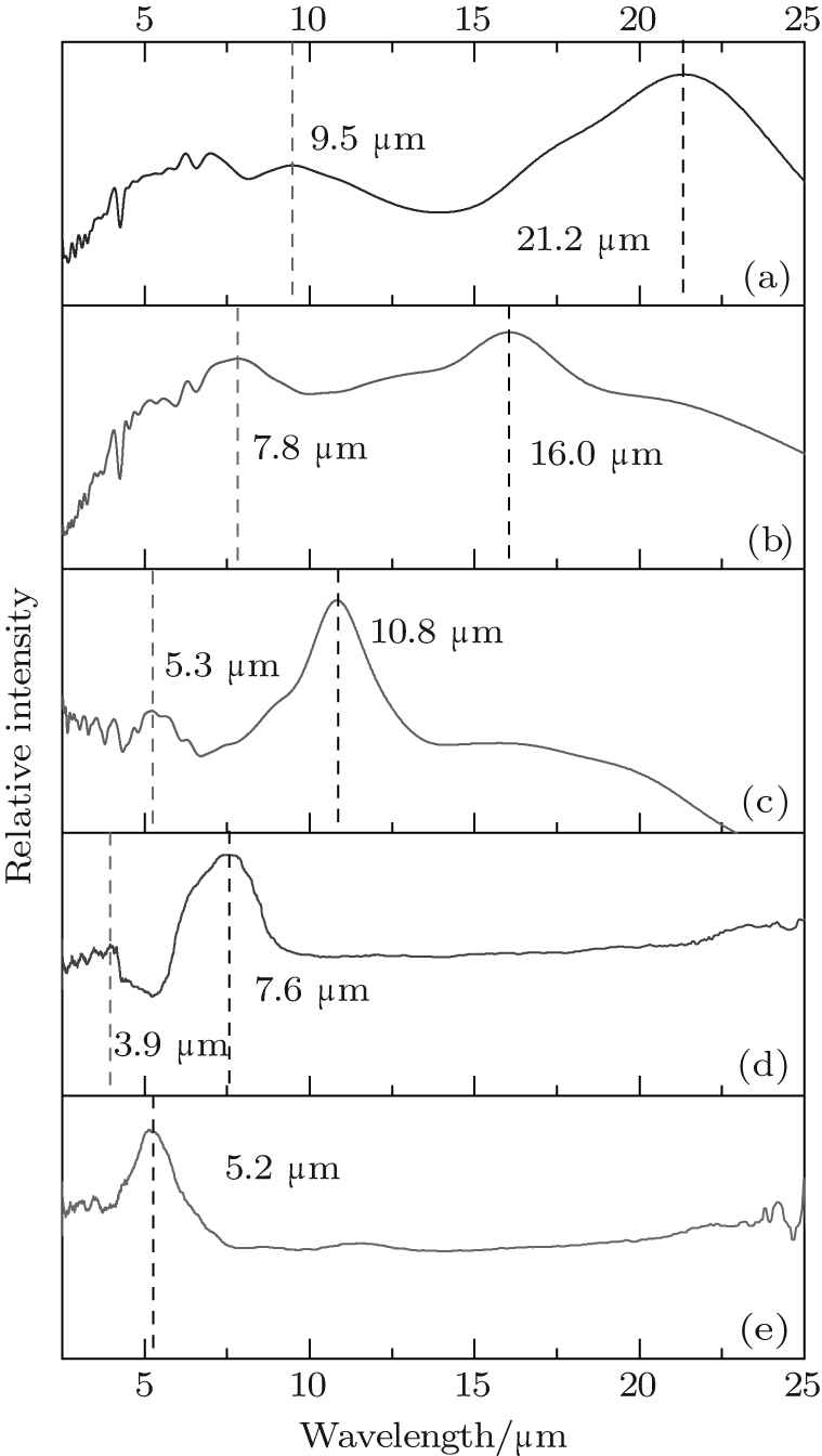 | Fig. 4. The relative intensity which is defined as dividing the normalized intensity of thermal radiation on the grating surface by the intensity on the polished surface, is plotted to observe the half wavelength of the enhanced peak easier. (a)– (e) 20 μ m, 15 μ m, 10 μ m, 7 μ m, and 5 μ m, respectively. |
In conclusion, fabricating a 1D surface grating pattern on a nickel surface can enhance its thermal radiation at the characteristic wavelength. In this experiment we process several period grating patterns on nickel targets through femtosecond laser direct writing. At grating periods 5 μ m, 7 μ m, 10 μ m, 15 μ m, and 20 μ m, we measure their thermal radiation spectra with an FTIR spectrometer at 623 K. The major enhanced peak wavelengths are 5.2 μ m, 7.6 μ m, 10.8 μ m, 16.0 μ m, and 21.2 μ m, respectively. We observe the half wavelength peaks of 3.9 μ m, 5.3 μ m, 7.8 μ m, and 9.5 μ m at major enhanced peaks at 7.6 μ m, 10.8 μ m, 16.0 μ m, and 21.2 μ m. The numerical simulation is shown by applying RCWA and Kirchhoff’ s law on thermal radiation. The simulation results show a good agreement with the experiment data. This paper implies that the laser fabricating technology can manipulate thermal radiation spectrally in a simple way. This technology shows potential applications on heat dissipation, infrared stealth technologies, etc.
| 1 |
|
| 2 |
|
| 3 |
|
| 4 |
|
| 5 |
|
| 6 |
|
| 7 |
|
| 8 |
|
| 9 |
|
| 10 |
|
| 11 |
|
| 12 |
|
| 13 |
|
| 14 |
|
| 15 |
|