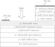
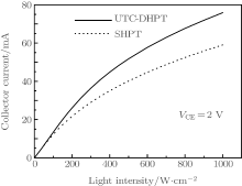
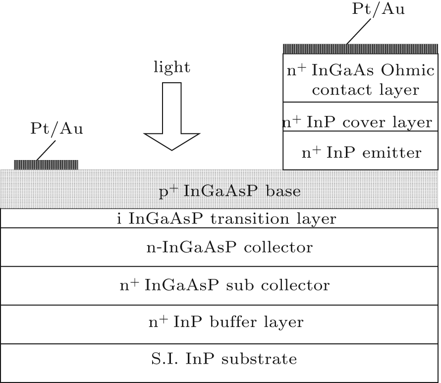
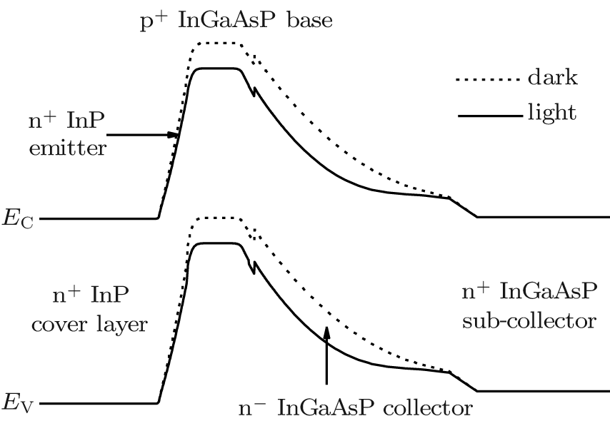
Analysis on high speed response of a uni-traveling-carrier double hetero-junction phototransistor*
Jiang Zhi-Yun, Xie Hong-Yun†, Zhang Liang-Hao, Zhang Wan-Rong, Hu Rui-Xin, Huo Wen-Juan
College of Electronic Information and Control Engineering, Beijing University of Technology, Beijing 100124, China

Corresponding author. E-mail: xiehongyun@bjut.edu.cn

*Project supported by the National Natural Science Foundation of China (Grant No. 61006044), the Natural Science Foundation of Beijing, China (Grant Nos. 4122014 and 4142007), and the Fund from the Beijing Municipal Education Committee, China (Grant No. KM200910005001).

Abstract

In this paper, the positive influence of a uni-traveling-carrier (UTC) structure to ease the contract between the responsivity and working speed of the InP-based double hetero-junction phototransistor (DHPT) is illustrated in detail. Different results under electrical bias, optical bias or combined electrical and optical bias are analyzed for an excellent UTC-DHPT performance. The results show that when the UTC-DHPT operates at three-terminal (3T) working mode with combined electrical bias and optical bias in base, it keeps a high optical responsivity of 34.72 A/W and the highest optical transition frequency of 120 GHz. The current gain of the 3T UTC-DHPT under 1.55-μm light illuminations reaches 62 dB. This indicates that the combined base electrical bias and optical bias of 3T UTC-DHPT can make sure that the UTC-DHPT provides high optical current gain and high optical transition frequency simultaneously.

Keyword: 85.60.Dw; 85.60.Gz; 78.55.Cr; 78.20.Bh; uni-traveling-carrier; double hetero-junction phototransistor; optical responsivity; optical transition frequency
1. Introduction

Hetero-junction phototransistors (HPTs) have attracted much attention because of their potential benefits in optical fiber communication and in millimeter-wave radio-over-fiber (ROF) systems. In ROF systems, HPTs not only serve as the high-performance photo-detector part but also amplify or mix microwave or millimeter-wave sub-carrier.[13] Most of the HPTs reported in the past two decades were fabricated using the AlGaAs/GaAs, InGaP/GaAs or InP/InGaAs material structures, and always had one or two hetero junctions with the base region, the base/collector depletion region and the collector region as the absorption area. In the depleted zone between the base and collector, electron– hole pairs were generated and separated. The optic generated holes dismissed/drifted slowly from collector to emitter, which restricted the device high frequency performance and thus the photoelectric response speed.[47]

The uni-traveling-carrier (UTC) idea was first proposed and applied to a photo-detector (PD) to make only one carrier (the electron) across the base and collector junction area.[812] UTC-PD had a faster response speed, higher saturation current, and wider linear dynamic range than the traditional PD detector. Recently, there were several reports on applying the UTC idea to an InP-based hetero-junction phototransistor (HPT).[13, 14] However, the main work focused on structure optimization based on a two-dimensional (2D) simulation and some elementary experiments. Since the UTC structure is expected to greatly improve the performance of HPT, it is necessary to further study the working mechanism and optimization of UTC-DHPT deeply.

In this paper, the UTC-DHPT working mechanism and the positive influence of UTC structure on HPT performance, including optical responsivity and optical transit frequency, are illustrated in more detail. UTC-DHPT performances under different electrical biases, optical biases and combined electrical and optical biases are shown and analyzed to make the UTC-DHPT achieve high optical current gain and high optical transit frequency simultaneously. The rest of this paper is organized as follows. The device structure of UTC-DHPT is described in Section 2 and also the positive influence of UTC structure on UTC-DHPT performance is illustrated in this section. In Section 3, the direct current (DC) characteristics and high-frequency characteristics of a 6 μ m× 1 μ m UTC-DHPT under different biased conditions (electrical bias, two-terminal working mode, and three-terminal working mode) are shown and analyzed to achieve high optical current gain and high optical cut-off frequency simultaneously. Finally, the conclusions are given in the last section.

2. Working mechanism of DHPT with UTC structure
2.1. UTC-DHPT device structure

The device structure schematic and structure parameters of InP/InGaAsP UTC-DHPT are given in Table 1 and Fig. 1 respectively. High doping In0.53Ga0.47As material is used as an n-type ohmic contact layer, and high doping InP material is used as an n-type cover layer. A middle doping InP material is used as an emitter, a high doping InGaAsP layer with a band energy of 0.80 eV is used as a base and a middle doping InGaAsP layer with a band energy of 1.12 eV as a collector and sub-collector. There are two thin InGaAsP layers used as transition layers for reducing the energy gap in the collector/base junction. The use of the medium doping wide-gap emitter and high base doping levels results in a small base-capacitance. This UTC structure forms two hetero-junctions respectively at the emitter/base junction and collector/base junction, which differs from the conventional single hetero-junction HPT (SHPT) in which the In0.53Ga0.47As is always employed as both base and collector. Thus, in the UTC-DHPT structure, only the highly doping InGaAsP (0.80 eV) base region is used as an optical absorption layer, while the collector together with the sub-collector are used as the collection region.

Fig. 1. Device structure of the UTC-DHPT.

Table 1. Epitaxial-layer parameters of the UTC-DHPT.
2.2. Working mechanism of UTC-DHPT

As illustrated in Fig. 1, the incoming light of 1.55 μ m is injected into the exposed base mesa from a 6 μ m× 1 μ m optical window to avoid additional light power loss from contact layer absorption. The incident radiation on the UTC-DHPT penetrates through the top surface of the base and is absorbed in the base region. Electron– hole pairs are generated and separated only in the p-doped base region because a wider energy band in the collector ensures the incoming light transports through the collector with less or no absorption, which is different from the combined absorption in the base and collector region in conventional SHPTs. The parallel electric field dependence formula and the Shockley– Read– Hall model are used to simulate the mobility and recombination of carriers respectively, with the effect of velocity saturation on mobility, Auger recombination, bandgap narrowing, Fermi– Dirac statistics, and impact ionization further taken into account. The energy band diagrams of the UTC-DHPT in the dark and under light with Vce = 2 V are shown in Fig. 2. The photo-generated electrons diffuse across the p+ -InGaAsP absorption layer into the adjacent totally depleted n-InGaAsP collection layer, where they are swept by the reversely enhanced electric field to form the initial electron photocurrent. The photo-generated holes, as the majority carrier in the base, relax fast toward the emitter and accumulate at the base/emitter hetero-interface and then lower the base-emitter barrier potential, which allows a large number of electrons to be injected from the emitter to the collector and amplifies the initial electron photocurrent.[14] A great photocurrent gain can be achieved by this process. The phototransistor optical responsivity (A/W) is calculated to be[15]

where Popt is the power of the optical beam and Ip is the output current of the UTC-DHPT.

Fig. 2. Energy band diagrams of the UTC-DHPT in the dark and under light.

Note that the HPT is also characterized as a heterojunction bipolar transistor (HBT) with the photocurrent as base bias. Its optical transition frequency (fT) can be expressed as[15]

where τ ec is the total emitter-to-collector signal delay time and is expressed as

Here, tte is the emitter depletion layer charging time, τ b is the base transit time, τ oh is the optical generated hole transit time, τ d is the collector depletion layer transit time, τ c is the RC time constant of the collector junction, and τ tc is the collector depletion layer charging time.

In conventional SHBT, τ oh is expressed as

where WB + WC is the optical-generated hole diffusion distance, and DPE is the hole diffusion coefficient. τ oh is dominated in the total carrier delay time because of the hole slow diffusion coefficient. Fortunately for the UTC-DHPT, the photo-generated holes move in a dielectric relaxation process from the base toward the emitter, which is faster than hole diffusion-drift movement in conventional SHPTs.

For a base uniform doping UTC-DHPT, the base transit time is expressed as

where WB is the base width and DnB is the elctron diffusion coefficient. Because there is only one carrier (electron) diffusing fast across the base area, the high electronic mobility leads to an extremely short τ b and helps to improve the DHPT working speed.

τ te and τ tc, which become dominated when HPTs deal with high frequency signals, are always expressed respectively as

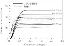
where CTE is the emitter transition capacitance, CTC is the collector transition capacitance, τ teCTE0/JC, CTE0 is the emitter transition capacitance per unit area, τ tcCTC0/JC, and CTC0 is the collector transition capacitance per unit area. For a UTC-DHPT and an SHPT with the same size, the UTC structure is of benefit to increasing the collector current and therefore the collector current density, as illustrated in detail in the following section. Thus it will reduce the charging times in the emitter/base junction and collector/base junction.

τ d is derived from the net space charge along with the change of collector current in the space charge area of the collector junction. Lower doping concentration of the collector region is conducible to optimizing τ d. τ c is proportional to the electrical resistivity and transition region capacitance per unit area as well as the width of the collector region. Therefore, τ d and τ c have weak dependences on UTC structure.

3. High speed response and discussion

The UTC-DHPT can operate under two working modes, i.e., the 2T working mode with an optical bias in the electrical floating base and the 3T working mode with a combined electrical and optical bias in the base. The dependences of Ic on the incident light intensity of both UTC-DHPT and SHPT are shown in Fig. 3. The optical beam having a light intensity in a range from 0 to 1000 W/cm2 is injected into the electrical floating base with the collector biased at Vce = 2 V. The UTC-DHPT is more suitable to dealing with a large-power light signal because the light-power intensities for UTC-DHPT and SHPT to become saturated are 300 W/cm2 and 100 W/cm2 respectively. The optical responsivity γ UTC-DHPT of UTC-DHPT is equal to 34.72 A/W according to Eq. (1). We also simulate the UTC-DHPT optical response under 3T working mode and obtain the same results because there is a voltage source applied in the base. Figure 4 shows the optical IV characteristics of UTC-DHPT and SHPT. It is apparent that the UTC structure makes a larger current gain than the SHPT structure. The reason is that the movement of an optical-generated hole in UTC-DHPT is accompanied with very fast dielectric relaxing and then makes a larger number of electrons enter into the base from the emitter in the same time period. This process results in higher emitter injection efficiency and a higher photocurrent gain.

Fig. 3. Variations of collector current of the UTC-DHPT and SHPT with incident light intensity.

Fig. 4. Output characteristic of the UTC-DHPT.

The dependences of transition frequency fT on Ic for 2T UTC-DHPT and 3T UTC-DHPT as well as the UTC-DHPT working as double heterojunction bipolar transistor (DHBT) are shown in Fig. 5. The dependences of the short circuit current gain (hfe) on frequency in these three operating conditions are shown in Fig. 6. All the collector biases in those three operating conditions have the same Vce = 2 V. Simulation results of the conventional SHBT and SHPT are also shown in Figs. 5 and 6.

Fig. 5. Dependences of fT on Ic of UTC-DHPT under 2T and 3T working modes.

Fig. 6. Short current gain dependences on frequency of UTC-DHPT under 2T and 3T working modes.

The curves in Figs. 5 and 6 show that when the DHPT is used as an electrical device, the transition frequency fT of the DHBT reaches a maximum value of 115 GHz as Ic is about 1.6 mA. When the DHBT operates at a common-emitter configuration with biasing conditions at Vce = 2 V and Vbe = 1.135 V, the short circuit current gain hfe of UTC-DHBT reaches 42 dB with a collector biasing current (Ic) of 2 mA.

The UTC-DHPT under 2T UTC-DHPT working mode operates by biasing the c– b junction negatively at Vce = 2 V with the optical injection of 1.55-μ m light into the base region. Maximum optical transition frequency fT of UTC-DHPT is about 80 GHz when Ic is about 24 mA, while the maximum hfe increases to 73 dB with a collector biasing current (Ic) of 4 mA. The attenuation of fT compared with the electrical biased DHBT results from the increases in emitter diffusion capacitance CDE and transition capacitance CTE as well as collector junction capacitance Cbc because the optically generated electrons and holes in the p-doped base region have a big influence on the inner carrier transportation. But the maximum fT of UTC-DHPT is still larger than that of conventional SHPT (about 60 GHz)[16] because the UTC structure breaks the speed limitation from slow mobility of holes. Therefore the UTC-DHPT has excellent frequency characteristics compared with the conventional SHPT. At the same time, maximum hfe of UTC-DHPT also benefits from UTC structure as illustrated above.

When the UTC-DHPT operates at the 3T working mode with the combined electrical bias and optical bias in the base, maximum optical transition frequency fT increases to 120 GHz at a collector biasing current of 30 mA and maximum hfe of the UTC-DHPT reaches 62 dB when the collector current is 7 mA (Vce = 2 V, Vbe = 1.135 V). This indicates that the combined base electrical bias and optical bias in 3T UTC-DHPT can make sure that the UTC-DHPT provides high optical cut-off frequency and high optical current gain simultaneously.

4. Conclusions

In this paper, the positive influences of UTC structure on HPT optical responsivity and high frequency characteristics are analyzed in detail. Benefiting from the single electron transportation of UTC structure, its optical responsivity reaches 34.72 A/W under the 2T working mode, and the maximum fT and maximum hfe of 2T UTC-DHPT under 1.55-μ m light illumination reach 80 GHz and 73 dB respectively, which are higher than those of a conventional single hetero-junction HPT. When the UTC-DHPT is biased by the combination of electrical biasing and optical biasing in the 3T working mode, a maximum cutoff frequency fT of about 120 GHz and a maximum current gain hfe of 62 dB are obtained, which proves that 3T UTC-DHPT can achieve a high working speed and a high optical current gain simultaneously. Therefore the UTC-DHPT designed in this paper exhibits the enhanced electrical and optical characteristics compared with the conventional single hetero-junction SHPT, and the 3T UTC-DHPT paves the way for future high-speed InP-based optoelectronic integrated circuits.

Reference
1 Polleux J, Paszkiewicz L and Billabert A 2004 IEEE Trans. M. T. T. 52 871 DOI:10.1109/TMTT.2004.823555 [Cited within:1]
2 Zhang S J, Wang H, Zou X H, Zhang Y L, Lu R G and Liu Y 2014 IEEE Photon. J. 6 5501008 [Cited within:1] [JCR: 2.356]
3 Khan H A and Rezazadeh A 2010 IET Optoelectron. 4 57 DOI:10.1049/iet-opt.2009.0011 [Cited within:1] [JCR: 0.849]
4 Tan S W, Chen W T and Chu M Y 2003 Superlattices and Microstructures 33 209 DOI:10.1016/S0749-6036(03)00079-X [Cited within:1] [JCR: 1.564]
5 Kosmas T, Bernard W and Ortwin H 2006 J. Phys. D: Appl. Phys. 39 1805 DOI:10.1088/0022-3727/39/9/016 [Cited within:1] [JCR: 2.528]
6 Beata S, Marek P and Artur B 2011 Central European Journal of Physics 9 1114 DOI:10.2478/s11534-011-0023-6 [Cited within:1] [JCR: 0.905]
7 Khan H A, Rezazadeh A A, Sohaib S and Tauqeer T 2012 IEEE J. Q. E. 48 576 DOI:10.1109/JQE.2012.2187176 [Cited within:1]
8 Zhang Y X, Liao Z Y and Wang W 2009 Chin. Phys. B 18 2393 DOI:10.1088/1674-1056/18/6/046 [Cited within:1] [JCR: 1.148] [CJCR: 1.2429]
9 Pan H, Li Z and Campbell J C 2010 J. Lightwave Technol. 28 1184 DOI:10.1109/JLT.2010.2043215 [Cited within:1] [JCR: 2.555]
10 Fu Y, Pan H and Li Z IEEE 2011 IEEE J. Q. E. 47 1312 DOI:10.1109/JQE.2011.2165700 [Cited within:1]
11 Rouvalis E, Chtioui M and vanDijk F 2012 Opt. Express 20 20090 DOI:10.1364/OE.20.020090 [Cited within:1] [JCR: 3.546]
12 Xue C L, Li C B, Liu Z, Cheng B W and Wang Q M 2013 Chin. Phys. B 22 118503 DOI:10.1088/1674-1056/22/11/118503 [Cited within:1] [JCR: 1.148] [CJCR: 1.2429]
13 Zhang S J, Zou X H, Zhang Y L, Zhang X X and Liu Y 2014 Microwave Opt. Technol. Lett. 56 427 DOI:10.1002/mop.v56.2 [Cited within:1]
14 Huo W J, Xie H Y and Liang S DOI:10.7498/aps.62.228501 2013 Acta Phys. Sin. 62 228501(in Chinese) [Cited within:2] [JCR: 1.016] [CJCR: 1.691]
15 Fukano H, Takanashi Y and Fujimoto M 1994 IEEE J. Q. E. 30 889 2895 [Cited within:2]
16 Kim J, Kanakaraju S and Johnson W B 2009 Electron. Lett. 45 649 DOI:10.1049/el.2009.0243 [Cited within:1] [JCR: 1.038]