Transient simulation and analysis of current collapse due to trapping effects in AlGaN/GaN high-electron-mobility transistor*
National Key Laboratory of ASIC, Hebei Semiconductor Research Institute, Shijiazhuang 050051, China
†Corresponding author. E-mail: xyzhoufly@163.com
‡Corresponding author. E-mail: ga917vv@163.com
*Project supported by the National Natural Science Foundation of China (Grant No. 61306113).
1. IntroductionGaN-based high-electron-mobility transistors (HEMTs) have attracted a lot of attention in the semiconductor community due to the potential capacity for next-generation high-frequency, high-temperature, and high-power electronic devices. Some successful GaN-based devices with excellent performance have emerged in the commercial market.[1] However, the advantages of these devices are limited by the radio frequency (RF) drain current collapse as well as other reliability problems.[2, 3] The presence of defects is considered to be the main cause of the parasitic effects. The defects can act as trapping centers to degrade the characteristics of devices. A lot of efforts and energy have been dedicated to the investigation of trapping phenomena.[4– 14] Pulsed I– V measurements are usually used to study the current collapse of GaN-based devices.[3– 6] In addition, transient techniques are very useful for identifying the traps in AlGaN/GaN HEMTs. The turn-on pulse transient tests and simulation with surface traps were carried out in Refs. [3] and [4]. The transient current response could not be explained with only surface donor traps, which was attributed to the interface acceptor traps.[7] The bulk trapping effect was analyzed with the transient simulation in Refs. [9]– [11]. Miccoli et al. contributed the gate-lag and drain-lag effects to the surface donor traps and the bulk acceptor traps, respectively.[14] Currently, two acceptable explanations for the mechanism of current collapse are the virtual gate theory with surface trapping and the hot-electron theory with bulk traps. However, the origin of traps is still under debate. Moreover, the traps may act as the donor/acceptor electron/hole traps. In the previous research work, traps were assumed to be at the surface, [3, 4] hetero-interface[7] or in the bulk (GaN buffer layer or AlGaN barrier layer).[8– 13] Our recent work investigated the influence of bulk acceptor traps in GaN buffer on the gate-lag transient characteristics of AlGaN/GaN HEMT.[15]
In this paper, based on the commercial Sentaurus TCAD software, [16] the two-dimensional (2D) numerical transient simulation work on the current collapse of Al0.3Ga0.7N/GaN HEMT in Ref. [17] is extended and discussed. By taking into account the coupling effect of traps and the thermal effect, the turn-on pulse transient current responses under different quiescent biases are obtained and the corresponding current collapses are observed. The mechanism of the current collapse can be explained by the trap occupation from the view of physics. The simulation results indicate that the bulk acceptor traps can influence the gate-lag transient characteristics besides surface traps and that the thermal effect may accelerate the emission of electrons for traps. Therefore, the bulk trapping effect on the gate-lag transient should be included for modeling the AlGaN/GaN HEMT to fit the real device characteristics more exactly. Furthermore, the pulsed current– voltage (I– V) curves are extracted from the transient simulation, showing a similar current collapse trend to the experimental pulsed I– V measurement results.
The rest of this paper is arranged as follows. In Section 2, the device structure and simulation model are described. The transient simulation results of Al0.3Ga0.7N/GaN HEMT are analyzed and discussed in Section 3. Finally, we conclude the paper in Section 4.
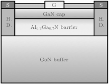
2. Description of device structure and modelThe schematic cross-section structure of the device used in our simulation is shown in Fig. 1. The gate with a length Lg = 90 nm is in the middle between the source and drain, whereas the source– drain distance is 2 μ m. The source and drain are both Ohmic contacts with heavily dopped (HD) regions. The hetero-structure is formed by a 2-μ m-thick undoped GaN buffer layer over an 18.5-nm-thick Al0.3Ga0.7N barrier layer. Moreover, a GaN cap layer with a thickness of 2 nm and an SiN passivation layer are adopted.
Unless otherwise specified, the parameter values for the simulation model are summarized in Table 1, and default values are used for other parameters not specified in the table. The Schottky barrier of the gate contact is set to be 0.9 eV in the simulation. The hydrodynamic transport equations are adopted instead of the drift-diffusion model to consider the role of hot electrons in the bulk trapping.[11] For the thermal effect, the thermodynamic model is included with a thermal contact at the bottom of the buffer, where the ambient temperature is set to be 300 K. Moreover, the electron mobility degradation model (i.e., high field saturation and doping dependence) and recombination mechanism (i.e., Shockley– Read– Hall, Auger and Radiative) are considered. Following the Sentaurus Device User Guide[16] and the work in Refs. [7], [18], and [19], the polarization effect is equivalent to the effect of fixed positive charges with a concentration of 1.3× 1013 cm− 2 at the Al0.3Ga0.7N/GaN interface. The surface donor traps with energy level Ed = 3.0 eV above the valence band (Ev) and bulk acceptor traps with energy level Ea = 0.5 eV below the conduction band (Ec) are taken into account in our simulation. The concentration of surface donor traps located at the interface of passivation/GaN cap layer is Nd = 3 × 1013 cm− 2, while the bulk traps uniformly distributed in the GaN buffer have a concentration of Na = 5 × 1016 cm− 3. It is assumed that the electron and hole capture cross sections of the traps are σ n, p = 1 × 10− 15 cm2.
Table 1.
Table 1.
 Table 1. Parameter values used in the simulation model.| Parameters | Values | Units |
|---|
| Schottky barrier for gate | 0.9 | eV | | Concentration of polarization charge | 1.3× 10¹³ | cm− 2 | | Electron mobility for 2DEG/buffer | 1990/1200 | cm2/(V· s) | | Asat for saturation velocity | 2× 10⁷ | cm/s | | Bsat for saturation velocity | 5.5× 10⁶ | cm/s | | Surface trap energy level Ed from Ev | 3.0 | eV | | Concentration Nd of surface traps | 3× 10¹³ | cm− 2 | | Bulk trap energy level Ea from Ec | 0.5 | eV | | Concentration Na of bulk traps | 5× 10¹⁶ | cm− 3 | | Capture cross section σ n, p | 1× 10− 15 | cm2 |
Note: Electron saturation velocity Vsat = Asat − Bsat · (T/300), where T denotes the lattice temperature (in units of K). | Table 1. Parameter values used in the simulation model. |
3. Transient simulation results and discussionIn this section, the simulation results of Al0.3Ga0.7N/GaN HEMT are discussed in detail. In our work, the pulse rise/fall time for the pulse voltage is set to be 20 ns.
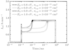
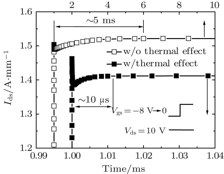
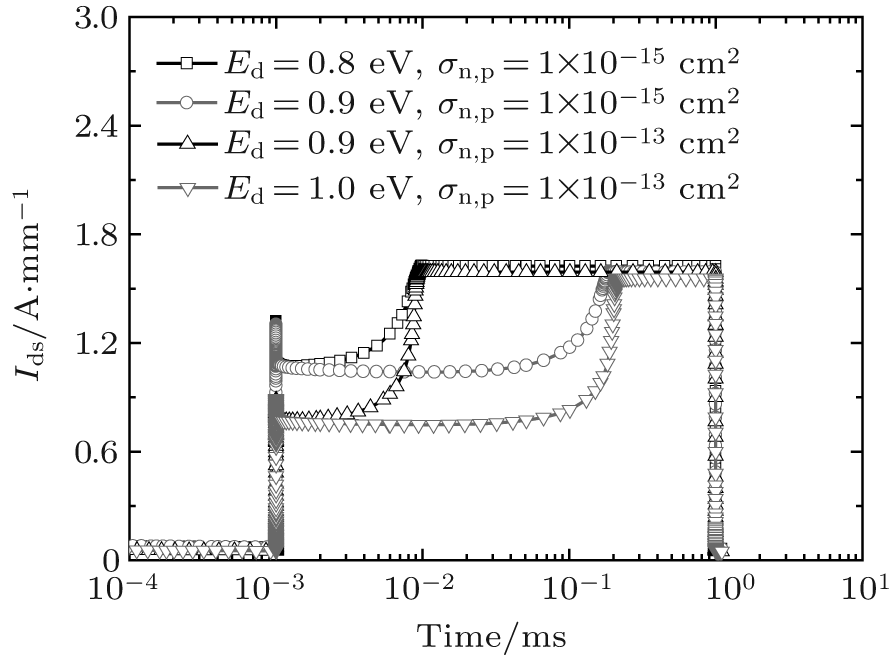
First, the simulated turn-on pulse gate-lag transient responses with and without the thermal effect are shown in Fig. 2. A transient voltage step is applied to the gate terminal with a fixed drain bias Vds = 10 V. Under this condition, the gate voltage is stepped from − 8 V (pinch-off situation for trap filling) to 0. The bottom axis in Fig. 2 corresponds to the current curve with the thermal effect (solid symbol), while the top axis is for the curve without the thermal effect (empty symbol). As seen from Fig. 2, the transient current rises with increasing time until it reaches the steady-state current, showing gate-lag current collapse. A similar phenomenon was also observed in the experimental measurement.[7] It has been proved that the gate-lag current collapse can result from surface donor traps.[3, 4] We also reproduce this phenomenon by the simulation with only surface donor traps, where the GaN cap layer is eliminated and the negative polarization sheet charge at the interface of the AlGaN barrier/passivation layer is included, proving the influence of surface traps (see Fig. 3, the surface trap energy Ed refers to the conduction band for this simulation). However, except the result in Fig. 3, since the negative polarization charge at the interface of the AlGaN barrier/GaN cap layer is not taken into account in this work, the surface trapping effect will not manifest itself according to the virtual gate theory. Therefore, the current collapses are mainly due to the bulk acceptor traps, and we have investigated the bulk trapping effect on the gate-lag transient of AlGaN/GaN HEMT.[15] In other words, bulk traps also played an important role in the gate-lag transient characteristics of AlGaN/GaN HEMT, which cannot be eliminated by passivation and should be considered in the model development of these devices. Moreover, an interesting phenomenon is found from Fig. 2, i.e., the rising time of the transient current with the thermal effect is shorter (∼ μ s) than that without the thermal effect (∼ ms). This indicates that the thermal effect may play a part in accelerating the emission of electrons for traps.
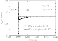
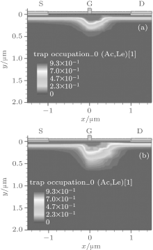
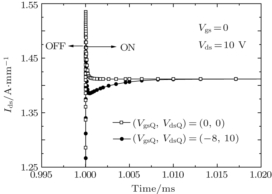
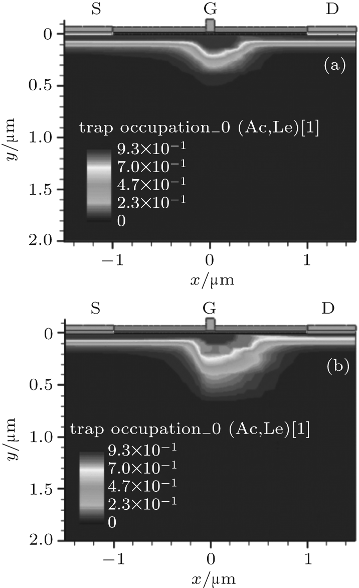
The thermal effect exists in the practical devices and influences their electric characteristics. Therefore, we take the thermal effect into account in all the following simulations. The transient currents of Al0.3Ga0.7N/GaN HEMT with different quiescent biases are plotted in Fig. 4. In this simulation, the device is first set to be the pinch-off situation with different quiescent bias points (VgsQ, VdsQ) and then turns into an open-channel state (Vgs = 0, Vds = 10 V). The current manifests a rising trend in the case of VgsQ = − 8 V and VdsQ = 10 V compared with in the case of VgsQ = 0 and VdsQ = 0 (see Fig. 4). This can be explained from the view of physics with the bulk trapping effect in the GaN buffer. The trap occupation maps for different cases at t = 1 μ s after turning on the device are shown in Fig. 5. It is obvious that traps deep in the GaN buffer are occupied by the electrons for the second case (VgsQ = − 8 V, VdsQ = 10 V), i.e., electrons are captured by the bulk traps deep in the buffer [see Fig. 5(b)]. Therefore, the corresponding current collapse is observed. However, the captured electrons are partially emitted by the traps with the time increasing, leading to the increase of transient current (Fig. 4).
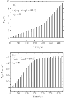
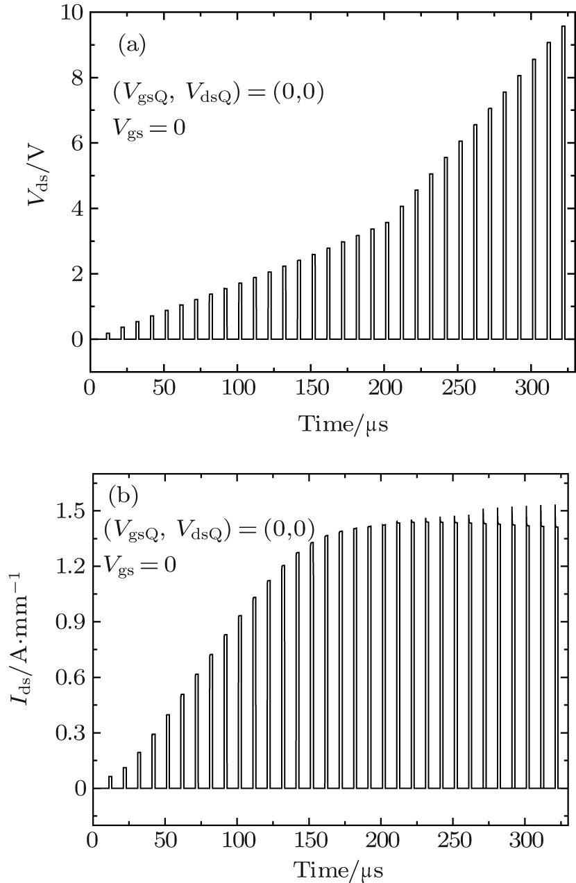
With the purpose of investigating the current collapse observed in the pulsed I– V measurement, the pulse transient simulation results of Al0.3Ga0.7N/GaN HEMT with different drain voltages are illustrated in Fig. 6. The pulsed drain voltage and the corresponding pulse transient current are shown in Figs. 6(a) and 6(b), respectively. The device is biased at VgsQ = 0 and VdsQ = 0 for the pinch-off state, while the gate voltage remains at 0 for the open-channel condition. The pulse width of 2 μ s and pulse period of 10 μ s are used. Based on this simulation, the pulsed I– V measurement result for studying current collapse can be reproduced as discussed below.
For comparison, the pulsed transient simulation with stress during the pinch-off situation is also carried out (Fig. 7). In this case, the device is biased at VgsQ = − 8 V and VdsQ = 10 V for the pinch-off situation. It can be seen from Fig. 7 that the current with VgsQ = − 8 V and VdsQ = 10 V is smaller than with VgsQ = 0 and VdsQ = 0. This is because the pulse width is not long enough for the current recovering, i.e., there is not enough time to detrap the captured electrons. If enough time is given, the final steady-state currents will achieve the same level for the two cases as shown in Fig. 4.
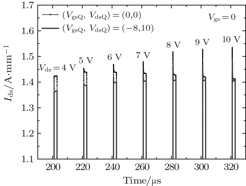
Furthermore, the pulsed I– V curves are extracted from the transient results with a pulse width of 400 ns and pulse period of 10 μ s. The experimental pulsed Ids– Vds curves of a passivated AlGaN/GaN HEMT device are given in Fig. 8(a), and the simulated corresponding characteristics of Al0.3Ga0.7N/GaN HEMT are illustrated in Fig. 8(b). It is observed that current collapse can be minimized but cannot be eliminated completely by passivation due to the existence of bulk traps. Additionally, the simulation result shows a similar trend to the experimental result. Moreover, the current collapse at Vds = 4 V near the knee point is larger than at Vds = 10 V for both the experimental and simulation results. In order to explain this phenomenon, a comparison of the simulated transient current response between Vds = 4 V and Vds = 10 V is made as shown in Fig. 9. The corresponding vertical electric field (Ey) along the y direction at x = 0.1 μ m for the time t = 1 μ s is shown in the inset. The lattice temperature is kept at 300 K for this simulation to exclude the influence of the thermal effect. As seen from Fig. 9, the current collapse at Vds = 4 V is larger and the current rising time is longer than at Vds = 10 V. This is because the vertical electric field at Vds = 10 V is too much larger than Vds = 4 V [see Fig. 9(b)], which can help the trapped electrons in the buffer return to the channel quickly.
4. ConclusionsIn this paper, the transient simulations of AlGaN/GaN HEMT are carried out and analyzed to investigate the current collapse, taking into account the coupling effect of trapping and the thermal effect. The simulation reproduces the experimental results of both the gate-lag transient current and the pulsed I– V curve. In addition, simulation results indicate that bulk acceptor traps can influence the gate-lag transient characteristics besides surface traps. Moreover, the thermal effect may play a role in accelerating the emission of electrons for traps. Pulse transient simulation is helpful for analyzing the dynamic current collapse. The work in this paper may be conducible to the reliability study and model development of GaN-based devices. The influence of traps with different properties (e.g. space location, trap energy level, and capture cross section) and method of reducing current collapse will be studied in our future work.


 , Feng Zhi-Hong‡