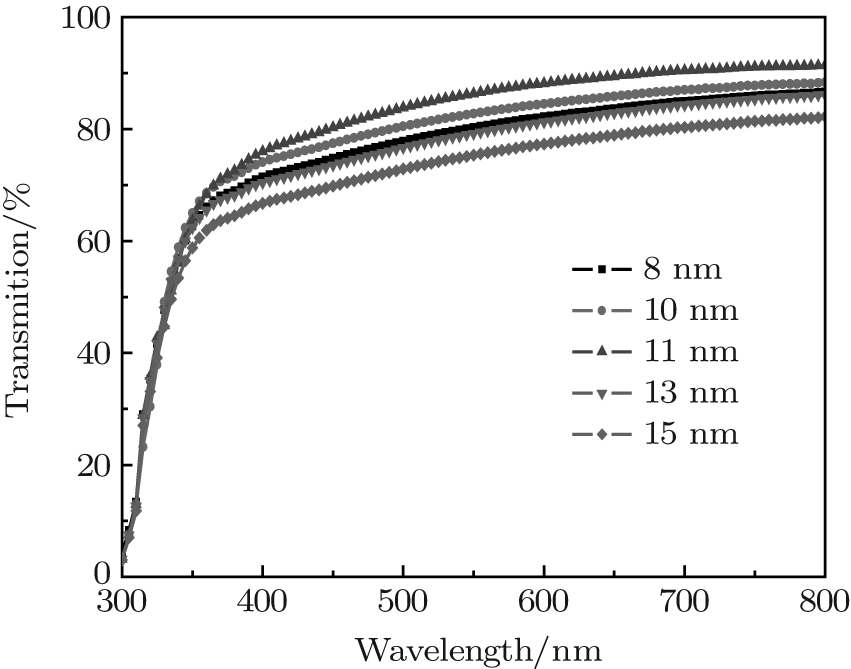
3.1. Influence of Cu thickness on photoelectric properties of TiO2/Cu/TiO2 multilayer film Figure 2 shows optical transmittance spectra in a wavelength range of 300 nm– 800 nm for multilayer films with different thickness values of Cu layers. The maximum optical transmittance of the pure single-layer TiO2 film is about 90% in the visible region. Although metal Cu has a high reflectivity, very thin films (< 15 nm) show moderate transmittances in the visible region and the top dielectric layer helps to obtain a higher transparent effect by diminishing the reflection from the metal layer.[15] As seen in Fig. 2, the optical transmittance of the multilayers increases as the Cu layer thickness increases from 8 nm to 11 nm. At a Cu thickness of 11 nm, the highest average transmittance of 86% in the visible spectral range is observed; this can be attributed to the evolution of the Cu layer, since Cu film with a thickness of less than 11 nm will have an island-shaped discontinuous micro-structure. The optical transmittance properties of the films can be understood in terms of the change in complex dielectric function for copper. In a discontinuous Cu film, a size-dependent variation in the dielectric function is known to exist due to the limitation of the mean free path of the conduction electrons. This leads to a correction to the imaginary part of the overall dielectric function (ε R) given by[16]

where ε m is the dielectric constant of the bulk metal, C is a constant at a particular wavelength, and R is the particle radius. As a consequence, below the critical thickness, as the radius of the Cu island decreases, the transmittance decreases. As Cu thickness increases, the Cu becomes a continuous layer from discontinuous islands, which causes a decrease in light scattering. However, further increasing Cu thickness above 11 nm results in an abrupt decrease in transmittance from ∼ 86% to 73% for 15-nm-thick Cu layer due to the increase in plasmon absorption and reflectivity of the mid-Cu layer, although we note that the augment of Cu layer thickness can increase the effective resistivity of the multilayer film. Thus, the appropriate thickness of the Cu layer is necessary for achieving maximum transmittance. It is found that the optimum value of Cu layer thickness is 11 nm with an average transmittance of 86% in the visible spectral range.
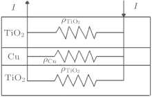
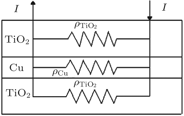
Figure 3 shows a parallel resistance circuit model of TCT multilayer film. The thickness of the Cu layer varies from 8 nm to 15 nm. The total resistance of the multilayer is a combination of the resistances of three consecutive layers, connected in parallel, and expressed as follows:[17]

The value of RCu is much less than TiO2 resistance, so the total resistance R ≈ RCu and the total resistance depends mainly on the Cu layer. We know that a thin Cu film growing on a crystalline bottom layer follows the Stranski– Krastanov[18, 19] growth mechanism of a layer plus-island growth model while Cu film growing on an amorphous TiO2 surface should follow the island growth mechanism of the Volmer– Weber model.[19] On the basis of island growth, we expect the different conduction mechanisms[20] before and after the critical thickness of the Cu middle layer. It has been proposed that in the case of continuous Cu film, when the islands are connected, there will only be metal conduction; however, in the case of discontinuous metal film with islands, there will be a different resistance model which includes: metal conduction, dielectric conduction, and quantum tunneling. Here, the surface coverage of the discontinuous Cu thin film will take a predominant role in the conduction among dielectrics (metal oxides) or quantum tunnelings.
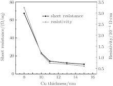
The four-point probe method is used for sheet resistance measurements. By using the four-point probe method, the semiconductor sheet resistance can be calculated from the following equation

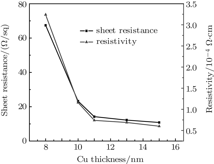
where V is the voltage reading on the voltmeter, I is the current carried by the two current-carrying probes. The sheet resistance is defined by RS = ρ /d, where ρ is the resistivity in Ω · cm and d is the coating thickness in cm. Figure 4 indicates the sheet resistance and resistivity of TCT multilayer film depending upon the thickness of the Cu layer. TiO2 is an insulator with a resistivity on the order of 107 Ω · cm. On depositing an 8-nm Cu film between the TiO2 layers, the resistivity decreases to 3.2× 10− 4 Ω · cm which suggests that there is an 11-fold decrease in resistivity in the TCT multilayer when compared with that in bare TiO2. As the effective Cu thickness increases from 8 nm to 15 nm, the multilayer resistivity decreases gradually down to 4.9× 10− 4 Ω · cm. As seen in Fig. 4, the resistivity of TCT multilayers drops rapidly from 8 nm to 11 nm, because the Cu film with a thickness of less than 11 nm has an island-shaped discontinuous micro-structure, which is not well conductive. As the islands grow, the separation between the islands decreases and some of the islands coalesce to form a continuous layer. This leads to a radical drop in resistance. However, as the Cu layer thickness further increases above 11 nm, the effective resistivity of the multilayer with the TCT multilayer gradually decreases and approaches to the resistivity of bulk Cu. The change in effective resistivity of the TCT multilayer film with increasing the Cu thickness can be explained by the following basic relationship:[21]

where ρ is the resistivity, n is the number of charge carriers, e is the charge of the carrier, and μ is the mobility. From this equation, we see that changes in mobility and carrier concentration can both affect the resistivity. When the Cu islands form a contiguous layer, the decrease in resistivity is governed by the combined effect of the increase in carrier concentration of conducting electrons and mobility.[22]
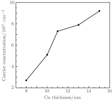
Figure 5 shows the change in carrier concentration with Cu thickness for TCT multilayer film. The plot indicates that the carrier concentration depends strongly on Cu thickness. The carrier concentration of the TCT multilayer films increases from 2.7× 1021 cm− 3 to 9.2× 1021 cm− 3 as effective Cu thickness increases from 8 nm to 15 nm. Hence, metallic conduction is dominant in this TCT system. There are many scattering mechanisms which can affect the mobility of carriers, and hence the resistivity of the film. Given that the conduction in the multilayer is primarily through the Cu mid-layer, the main scattering mechanisms that can influence charge carriers are interface scattering, surface scattering, or grain-boundary scattering.
A figure of merit, (as defined by Haacke) is estimated for each of the TCT multilayers using the following relationship

where Tav is the transmittance and Rsh is the sheet resistance. The multilayer with a mid-Cu thickness of 11 nm (T: 86% and Rsh: 14.2 Ω /sq) has a maximum figure of merit of 15.6× 10− 3 Ω − 1.
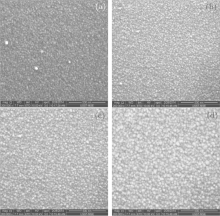
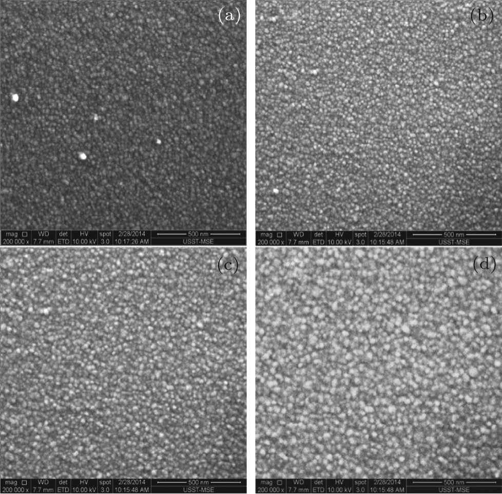
3.2. Influence of annealing temperature on photoelectric properties of TiO2/Cu/TiO2 multilayer film In order to examine the thermal stabilities of the properties of multilayer films, TiO2/Cu(11 nm)/TiO2 multilayers are annealed at different temperatures (150 ° C ∼ 400 ° C) in air. Figure 6 shows the SEM morphological images of TiO2/Cu(11 nm)/TiO2 multilayer films annealed at different temperatures. As can be seen from the images, with increasing the annealing temperature, the grain size of TiO2 increases and the uniformity is improved. Annealing treatment can change the surfaces of films more homogeneously with better coverage and reduction of the porosity of the films. This is consistent with the result of the crystalline properties. At high temperature, the atoms have enough diffuse activation energy to occupy the correct site in the crystal lattice and grains with the lower surface energy will become larger at high temperature.[23]
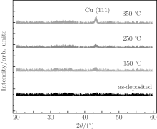
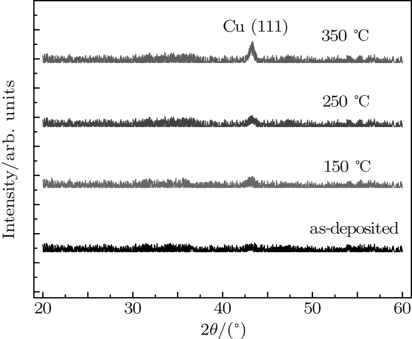
The crystalline structures of different multilayer films are determined by XRD measurements. Figure 7 shows the XRD patterns of the as-deposited TiO2/Cu(11 nm)/TiO2 multilayer films and post-deposition annealed films at different temperatures respectively. It is seen that in each XRD pattern there exists only the Cu (111) peak, but no apparent titanium dioxide crystalline peaks appear. As-deposited TiO2/Cu (11 nm)/TiO2 films do not show any strong diffraction peaks in the XRD patterns; this is due to the low substrate temperature and film being too thin to form a crystalline phase. Upon increasing the annealing temperature to 150 ° C, the TiO2/Cu(11 nm)/TiO2 multilayer starts to show a crystalline Cu (111) peak at 43.3° . The intensity of the Cu (111) peak increases with annealing temperature rising. This finding can be understood based on the fact that the thermal energy during annealing may enable atoms to diffuse and stack. As a result, the number of deposition defects is reduced and a more perfect crystal structure is formed.[24]
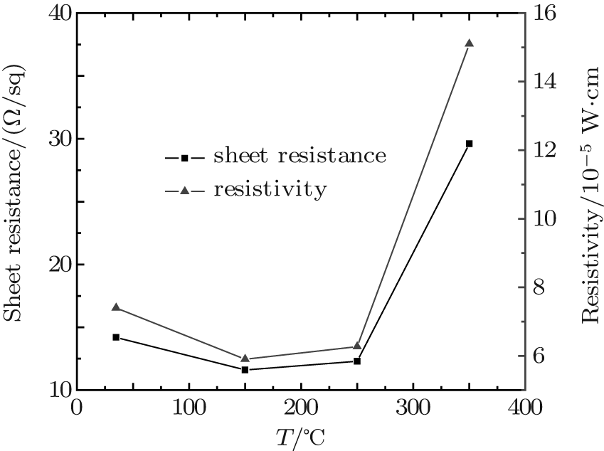
Figure 8 indicates the effects of annealing on the sheet resistance and resistivity of the TiO2/Cu(11 nm)/TiO2 multilayer film. The resistivity of the as-deposit film is 7.4× 10− 5 Ω · cm. It decreases slightly with temperature until 150 ° C, where the resistivity has a highest value of 5.9× 10− 5 Ω · cm, which is attributed to the improved crystal quality of TiO2 film and efficient protection from forming Cu-oxide.[25] However, with further increase of annealing temperature, the sheet resistance increases, and the resistivity of the TiO2/Cu(11 nm)/TiO2 multilayer increases drastically to 1.51× 10− 4 Ω · cm at an annealing temperature of 350 ° C. For such a deterioration, two primary reasons have been found: one is an agglomeration of Cu film during annealing, which leads to the sheet resistance increase by the enhanced surface scattering effect; [26] the other is that the effective thickness of the Cu layer becomes thinner. The Cu has a high diffusion coefficient and it can migrate quickly into the TiO2 film in the heat process and the effective thickness of the Cu layer becomes thinner. Therefore, the resistivity increases as temperature further increases. While the annealing temperature is above 400 ° C, the resistivity of the multilayer film becomes very high, almost as high as an insulator resistivity. This can be attributed to the oxidation of the Cu layer, when the heat treatment takes place in air, an oxygen atom in the air diffuses through the TiO2 layer and oxidizes the Cu layer partly.
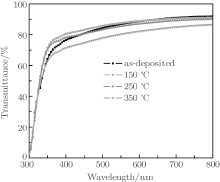
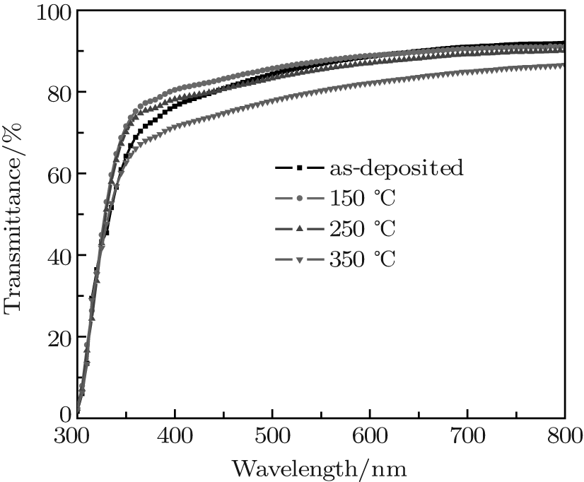
Figure 9 shows the effects of annealing on the transmittance of the TiO2/Cu(11 nm)/TiO2 multilayer films. It is observed that the optical transmittance increases with the increase of annealing temperature up to 150 ° C. The TiO2/Cu(11 nm)/TiO2 multilayer with 150- ° C annealing temperature shows a maximum average optical transmittance of around 88%. With the further increase of annealing temperature, multilayer performance decreases. This phenomenon can be explained as follows. Because of the better crystallization degree of TiO2 (Fig. 6), there are fewer grain boundaries, which will reduce the scattering of incident light. As a result, the transmittance increases. However, with further increasing the annealing temperature, on the one hand, the surface roughening due to agglomeration of Cu film during annealing results in more scatterings of the incident light and decreasing of transmittance.[27] On the other hand, diffusion of Cu atoms onto the TiO2 film by annealing may reduce the antireflection effect of the TiO2 film due to the higher optical absorption of Cu atoms, resulting in lower optical transmittance.[28]


 , Kou Zhi-Qi, Wang Li-Jun, Wang Jin-Ye, Sun Yi-Qing]