

Tunable coplanar waveguide resonator with nanowires*
[Zhou Yu, Jia Tao, Zhai Ji-Quan, Wang Cheng, Zhong Xian-Qian, Cao Zhi-Min, Sun Guo-Zhu† , Kang Lin, Wu Pei-Heng]
, Kang Lin, Wu Pei-Heng]
|
|

 , Kang Lin, Wu Pei-Heng
†Corresponding author. E-mail: gzsun@nju.edu.cn
*Project supported by the National Basic Research Program of China (Grant Nos. 2011CB922104 and 2011CBA00200), the National Natural Science Foundation of China (Grant No. 11474154), the Jiangsu Natural Science Fund for Distinguished Young Scholars (Grant No. BK2012013), and a Doctoral Program (Grant No. 20120091110030).
A tunable superconducting half-wavelength coplanar waveguide resonator (CPWR) with Nb parallel nanowires ∼ 300 nm in width embedded in the center conductor was designed, fabricated, and measured. The frequency shift and the amplitude attenuation of the resonance peak under irradiation of 404-nm pulse laser were observed with different light powers at 4.2 K. The RF power supplied to such a CPWR can serve as current bias, which will affect the light response of the resonator.
In the past few years, superconducting coplanar waveguide resonators (CPWRs) have been intensely studied and applied to the field of superconducting quantum bits, [1, 2] transforming cavity quantum electrodynamics (QED) into circuit QED, [3– 5] in which superconducting CPWRs are used as tools to measure the quantum states of quantum bits. Moreover, a CPWR can also function as “ a quantum bus” to mediate the coherence between quantum bits.[6, 7] To mediate the quantum bits, the resonator needs to be tunable. Many researchers use lossless Josephson junctions as tunable components to tune the resonance frequency.[8, 9] Actually, changes in some of the electromagnetic parameters of CPWRs may cause variation of the resonant frequency and/or the resonant amplitude. So there may be other ways to achieve a tunable resonator. On the other hand, for superconductors, the photons with energy hν > 2Δ can break the Cooper pairs into quasiparticles, which changes the surface impedance Zs of the superconductors. Zs has two components:

In superconductors, Ls is dominated by the kinetic inductance Lk, which varies with the density of Cooper pairs. Microwave kinetic inductance detectors (MKIDs) can detect photons by monitoring the change in the resonance frequency of CPWRs caused by alteration in the kinetic inductance of superconductor thin film after absorbing photons, so they are now being applied in astronomy for optical/UV/x-ray detection.[10– 12] A different photon detection approach using CPWRs with structure similar to that that of MKIDs has also been reported.[13] Another promising optical detector in the superconducting field is the superconducting nanowire single photon detector (SNSPD), [14, 15] which is biased near but below the critical current, using the variation of Rs in nanowires after photon absorption to detect photons. Due to its nanometer scale geometry, such a detector can respond to very weak light, even one photon. Although the detection mechanisms of MKID and SNSPD are different, the interaction of photons and Cooper pairs occurs in both.
According to our previous work on SNSPDs, [16, 17] it is promising that inserting nanowires into the CPWR may result in a tunable superconducting resonator, much like combining MKID and SNSPD. Note that here we use light to tune the CPWR with nanowires instead of using CPWR to detect photons.
The resonance frequency of a half-wavelength CPWR on a single layer substrate is given by[10]

where n is the mode number, c is light velocity in a vacuum, ɛ is the relative dielectric constant of the substrate (for silicon, ɛ = 11.9), and L is the length of the CPWR.
The main geometric parameters of CPWRs are shown in Fig. 1. The fundamental resonance frequency is designed to be 7.5 GHz. So the total length of the CPWR is L = 7880 μ m. We chose the width of the center conductor w = 26 μ m, for the consideration of a relatively large optical illumination area and an easier fabrication process. The substrate is high resistivity silicon with thickness h = 350 μ m. In order to reduce loss, the material chosen for the CPWR is niobium (Nb) film with thickness t = 300 nm. To ensure a 50-Ω impedance, the LineCalc tool in ADS was used to calculate the distance between the center conductor and ground, s = 16 μ m.
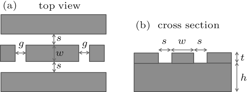 | Fig. 1. Geometry of a typical half-wavelength CPWR with gap capacitors: (a) top view, (b) cross section view. The center conductor and lateral ground (blue) are on top of a high resistivity silicon substrate (gray). |
The parameter g is relevant to the loaded quality QL of CPWRs. QL is determined by[8]

where Qint represents the internal loss of the resonators, including Ohmic loss and radiation loss, and Qc is for the coupling loss.
Qint is quite large, with a magnitude of at least 105, because the superconductor is lossless. To ensure a larger QL for small loss and narrow bandwidth, we should make Qc ≫ Qint, otherwise QL ≈ Qc . While Qc is mainly determined by the coupling capacitance, so it increases as the gap g is enlarged. However, if the gap gets too large, there is much insert loss in the S21 parameter, thus decreasing the SNR. For a half-wavelength CPWR, Qc can be calculated using 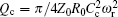
We also ran an HFSS simulation to validate the above parameters.
The kinetic inductance is due to the inertial mass of moving charge carriers in AC fields, and it will increase as the carrier density decreases. For superconductors, the carriers are Cooper pairs. The interaction between photons and Cooper pairs will affect the kinetic inductance of the superconductor and thus the surface impedance, finally bringing shift or loss to the resonance peak of the resonator.
We can calculate the kinetic inductance by equating the kinetic energy of Cooper pairs with the equivalent inductive energy:[19]

where I is the supercurrent in the superconductor, ns is the density of Cooper pairs, lwd is length× width× thickness of the superconductor, 2m represents the mass of a Cooper pair, and v is the average velocity of Cooper pairs. Substituting I = 2ns ev · (wd) into Eq. (4), we will obtain

With a specific superconducting material, the kinetic inductance is determined by its geometry size. We expect that a single nanowire can have large kinetic inductance. Moreover with the definite geometry of the CPW structure, the ratio α of the kinetic inductance Lk to the total inductance Ltotal will increase as the film thickness decreases, when the thickness is less than half of the magnetic penetration depth.[20] Meanwhile the internal quality Qint of the CPWR will decrease dramatically when the film thickness decreases. According to Ref. [11] the responsivity of the resonator is directly proportional to α QL / V, where V is the volume of the resonator. To ensure an observable change in the resonance peak, according to the London penetration depth of Nb, λ L (0) ≈ 44 nm, [21] 20-nm Nb film is chosen for the nanowires to make the QL at least several hundred at 4.2 K and α to be at least around 0.1 for both acceptable loss and observable response.
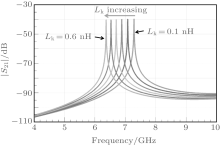
The nanowire remains in the center of the center conductor because the maximum current density is located in the center of the half-wavelength CPWR when in the fundamental mode. The kinetic inductance introduced by the nanowire structure will make the resonance peak shift from the original designed resonance frequency 7.5 GHz. The simulated results using the advanced design system (ADS), as shown in Fig. 2, show that the larger Lk is, the more right-to-left frequency shift there will be.
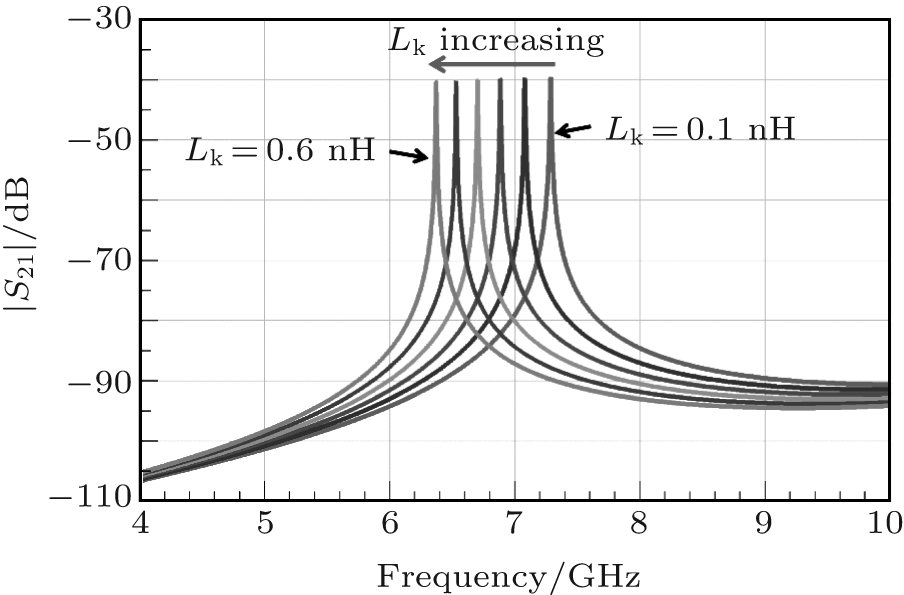 | Fig. 2. Simulation results of the fundamental resonance frequency with different kinetic inductances in the center conductor of a CPWR, using ADS. The kinetic inductance Lk increases from right to left by 0.1 nH per step and the minimum is 0.1 nH. |
To ensure that the fundamental resonance frequency of this CPWR is not far below 7 GHz, we chose a parallel structure to reduce the initial kinetic inductance. We designed six nanowires arranged in parallel, each ∼ 300 nm in width and 10 μ m in length, as shown in Fig. 4(b).
With a rough estimate, [19] we expect the total kinetic inductance to be around 0.1 nH.
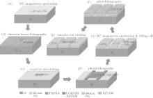
The CPWR with nanowires is fabricated by a process similar to that for SNSPDs.[22] The high resistivity silicon substrate is first cleaned following the standard cleaning procedure. Then Nb film with a thickness of ∼ 20 nm is deposited on the substrate using DC magnetron sputtering. Electron beam lithography (EBL) follows, to pattern the nanowire structure with a PMMA 950 A2 photoresist. After reactive ion etching (RIE) with SF6, the photolithography with LOR10B/AZ1500 is applied to pattern the CPWR structure on the thin film, and then Nb film with a thickness of ∼ 300 nm is deposited after Ar ion milling. A lifting off process is subsequently used to shape the CPWR structure. In the final step, a second photolithography process with AZ1500 and RIE process with SF6 are performed to remove the unneeded thin film between the center conductor and the ground of the CPWR. The specific fabrication process is shown in Fig. 3.
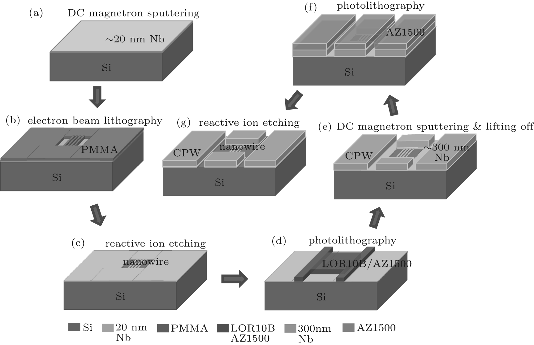 | Fig. 3. Main steps of the fabrication process, from (a) to (g): (a) DC magnetron sputtering to deposit the first layer of ∼ 20-nm Nb film; (b) electron beam lithography to pattern the parallel nanowires; (c) reactive ion etching to transfer the nanowires to the thin Nb film; (d) photolithography to make the mask for CPWR; (e) DC magnetron sputtering and lifting off to deposit the second layer of ∼ 300-nm Nb film for CPWR; (f) photolithography to make the mask for the unneeded thin film between the center conductor and ground; (g) reactive ion etching to remove the unneeded thin film between the center conductor and ground. |
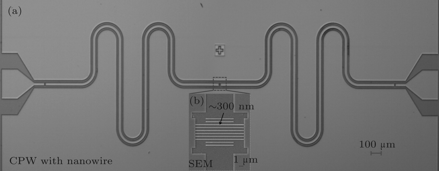 | Fig. 4. (a) Optical image of the half-wavelength CPWR with six parallel nanowires in the center conductor; (b) SEM image of six parallel nanowires in the center conductor. |
We perform the EBL in an early step rather than in a later step to avoid PMMA (thickness of ∼ 70 nm) unevenness in the center area (10 μ m× 10 μ m) during the spin coating process if ∼ 300 nm Nb film has been deposited, and to improve the quality of the nanowire simultaneously.
After the fabrication process, the samples are cut into 4.4 mm× 2.7 mm chips. A single chip is shown in Fig. 4(a).
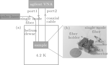
The sample is glued on the holder using Oxford GE Varnish and is wire bonded to a microwave PCB for the electrical connection. Our sample holders with four SMA connectors and a fiber holder component to align the single mode optical fiber are made of oxygen-free copper to ensure good thermal conductivity. The single mode fiber has a core diameter of 9 μ m and is also fixed in the fiber holder using Oxford GE Varnish. All the components are assembled with brass screws. The finished sample package after fiber alignment is shown in Fig. 5(b).
The finished sample holder is then attached to a measurement rod with coaxial cables and one FC/PC connector. We calibrate the two coaxial cables using a standard agilent vector network analyzer (VNA) calibration procedure at room temperature. The picosecond pulse laser (PPL) with 404-nm wavelength is connected to the single-mode fiber through an FC/PC connector. The equipped measurement rod is then inserted into a helium dewar. When the temperature is stable, two VNA microwave cables are connected to the SMA connectors on the rod to measure the S21 parameter of the sample. The specific measurement setup is shown in Fig. 5(a).
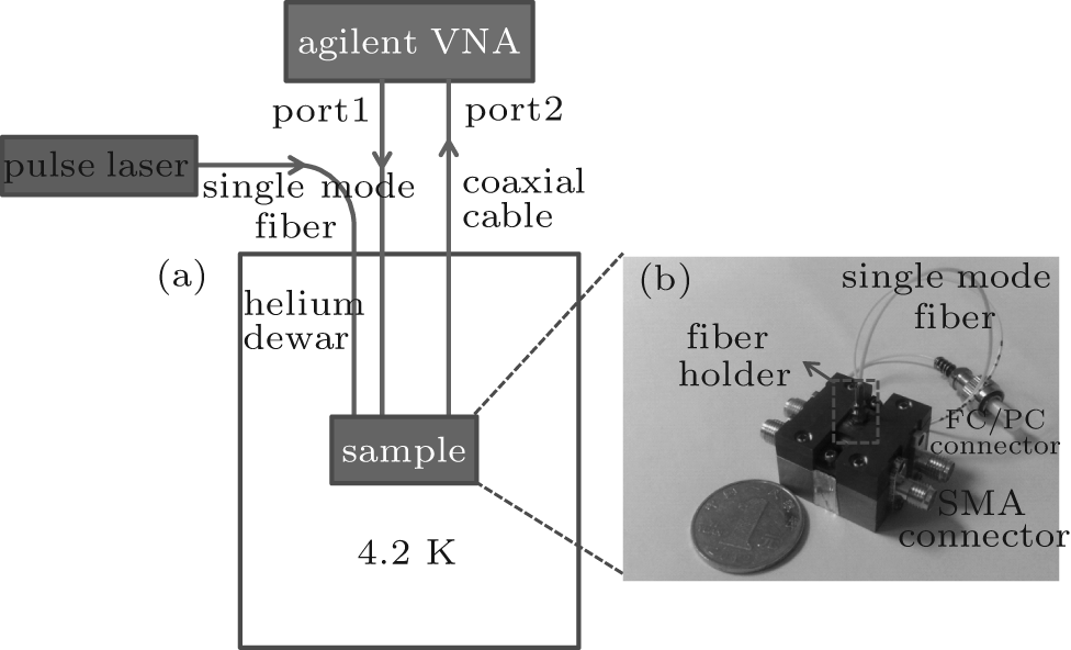 | Fig. 5. (a) Schematic diagram of the measurement setup; (b) sample package with optical fiber aligned. |
We measured the S21 parameters of our sample in the helium dewar at 4.2 K with different levels of RF power and different powers of incident light. The repetition rate of the 404-nm PPL is set to the maximum, 100 MHz.
The HFSS simulation of the surface current distribution on the nanowires at the source power of 10 dBm gives the maximum surface current density Jsurf ≈ 2× 10² A / m. This means the supplied RF power from VNA can serve as AC current bias in analogy to the DC bias in SNSPD and such induced AC current can affect the nanowires’ sensitivity to light. The difference between such induced AC current bias in nanowires of our sample and the DC bias in SNSPD is that the magnitude of the induced current will vary with time.
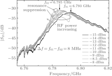
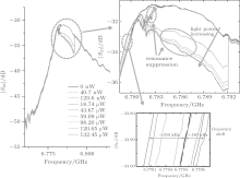
Under the irradiation of 404-nm PPL with constant optical power at 40.7 nW, we swept the S21 parameters at different RF power levels.
As shown in Fig. 6, with different levels of RF power, the S21 parameters have different shapes: 1) for low RF power (from − 15 dBm to − 9 dBm), only resonance frequency shifts occur and the sizes of the shifts correspond to the power level. 2) For RF power of − 8.5 dBm, a critical power level, besides the resonance frequency shift, a small resonance suppression also exists. 3) While for a still larger RF power level at − 8 dBm, resonance suppression becomes dominant, and when RF power is at − 9 dBm, the resonance peak, with the loaded quality QL = 440, is completely suppressed.
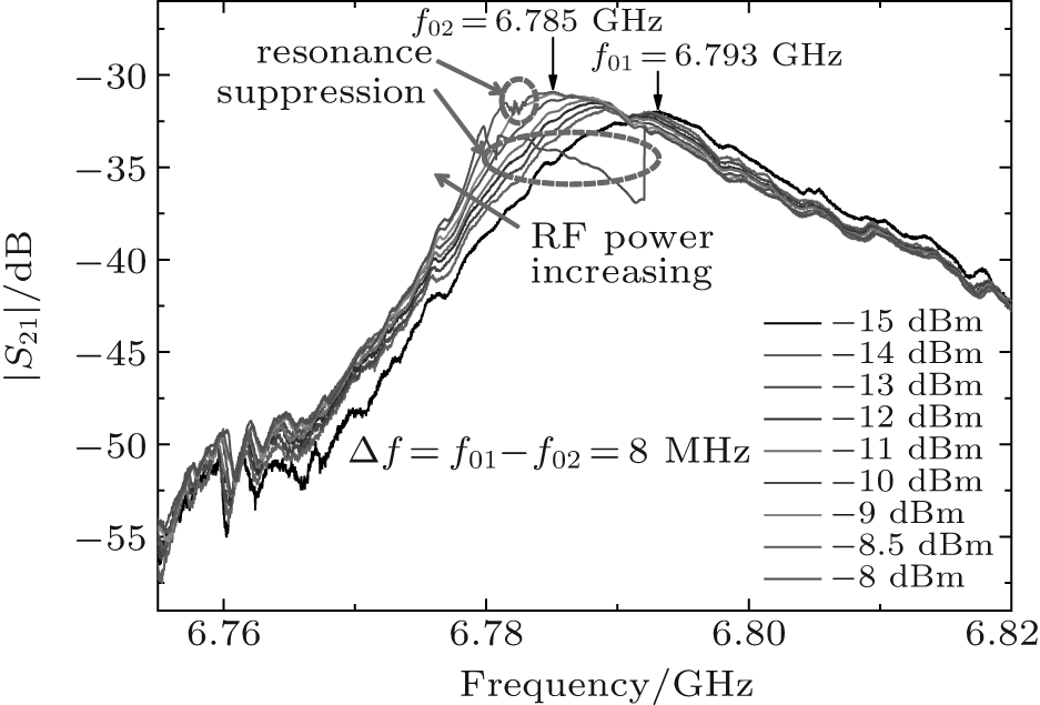 | Fig. 6. S21 parameters of the sample measured with the same optical power at 40.7 nW but different RF power levels ranging from − 15 dBm to − 8 dBm. Here f01 is the resonance peak measured with RF power at − 15 dBm, and f02 is the resonance peak measured with RF power at − 9 dBm. |
This is because with higher induced current, absorbed photons not only change the kinetic inductance but also transform part of the nanowire from the superconducting state into the normal state. Therefore, with the higher RF power, the nanowire will become more sensitive to incident light, resulting in magnitude suppression rather than a frequency shift in the resonance peak.
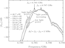
We then set the RF power of the VNA to a well-chosen level at − 8.6 dBm, which is near the critical power level, to measure the S21 parameters with 404-nm PPL at different incident optical powers. As shown in Fig. 7, when the optical power is low, the effect of resonance suppression is small. As the optical power increases, the suppression of the magnitude in the resonance peak becomes more obvious. As we mentioned above, the RF power from the VNA functions as the DC bias in SNSPD, and the value of − 8.6 dBm is expected to be quite close to the critical current of the nanowire. Thus for low optical power, the amount of broken Cooper pairs is small, leading to small Ohmic loss and little change in kinetic inductance. Higher optical power causes a larger amount of broken Cooper pairs and thus greater Ohmic loss and a greater change in kinetic inductance. In fact, increasing optical power may even make the nanowire non-superconducting. In such a situation, the magnitude suppression is dominant instead of the frequency shift.
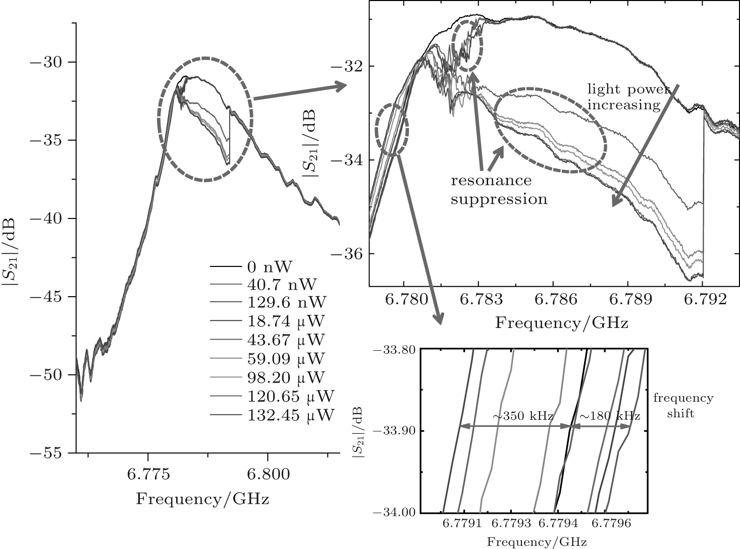 | Fig. 7. S21 parameters measured at different optical powers, ranging from 0 nW to 132.45 μ W. The RF power is − 8.6 dBm and the insets show the magnified details of the S21 parameters, measured with different optical powers. |
 | Fig. 8. S21 parameters measured at different optical power levels. The RF power is − 10 dBm. The f01 and f02 are the resonance peaks with optical power of 40.7 nW and 137.90 μ W, respectively. |
To explore the variation of resonance frequency shift with optical power, we set the RF power at − 10 dBm to avoid resonance suppression. As shown in Fig. 8, when the light power increases, corresponding to greater change in kinetic inductance, the resonance frequency shift also increases. The resonance frequency shift between the optical power levels of 40.7 nW and 137.90 μ W is about 2 MHz. The variation tendency is consistent with the simulation in Fig. 2.
Note that in the present measurement system, the tunability of the resonator is mainly due to Cooper pairs being broken in the nanowires by the heating effect of the optical power, because at 4.2 K the quasiparticle recombination time of Nb is less than 1 ns according to Ref. [23] which is much shorter than the repetition time of the optical source. In order to further investigate photon-induced Cooper-pair breaking, one has to decrease the temperature to get a longer quasiparticle recombination time and/or develop a new measurement system using heterodyne detection[11, 24] to obtain a quick response of the nanowires to photon injection.
We investigated the response of CPWR to light at the wavelength of 404 nm with different light power levels and observed resonance suppression and resonance frequency shift. The experimental results show that different levels of supplied RF power, serving as different AC current bias levels, also affect the response of the resonator to the incident photons. With low RF power, the response will be dominated by a resonance frequency shift. While with high RF power, resonance suppression will be more evident. These preliminary results should be helpful for further investigating an optically tunable CPWR with nanowires.
The author would like to thank Liu Xiao-Yu from the Shanghai Institute of Microsystem and Information Technology (SIMIT), the Chinese Academy of Sciences for the electron beam lithography and Gu Min for the beneficial discussion on sample fabrication.
| 1 |
|
| 2 |
|
| 3 |
|
| 4 |
|
| 5 |
|
| 6 |
|
| 7 |
|
| 8 |
|
| 9 |
|
| 10 |
|
| 11 |
|
| 12 |
|
| 13 |
|
| 14 |
|
| 15 |
|
| 16 |
|
| 17 |
|
| 18 |
|
| 19 |
|
| 20 |
|
| 21 |
|
| 22 |
|
| 23 |
|
| 24 |
|