


Perfect GMR effect in gapped graphene-based ferromagnetic–normal–ferromagnetic junctions
[Karbaschi Hossein† , Reza Rashedi Gholam]
, Reza Rashedi Gholam]
|
|


†Corresponding author. E-mail: h.karbaschi@sci.ui.ac.ir
We investigate the quantum transport property in gapped graphene-based ferromagnetic/normal/ferromagnetic (FG/NG/FG) junctions by using the Dirac–Bogoliubov–de Gennes equation. The graphene is fabricated on SiC and BN substrates separately, so carriers in FG/NG/FG structures are considered as massive relativistic particles. Transmission probability, charge, and spin conductances are studied as a function of exchange energy of ferromagnets ( h), size of graphene gap, and thickness of normal graphene region ( L) respectively. Using the experimental values of Fermi energy in the normal graphene part ( EFN ∼ 400 meV) and energy gap in graphene (260 meV for SiC and 50 meV for BN substrate), it is shown that this structure can be used for both spin-up and spin-down polarized current. The latter case has different behavior of gapped FG/NG/FG from that of gapless FG/NG/FG structures. Also perfect charge giant magnetoresistance is observed in a range of
As is well known, graphene is a two-dimensional monolayer of graphite.[1] Its unique properties are indicated to be an appropriate candidate for constructing electronic and spintronic devices.[2, 3] The carriers in the graphene fabricated on SiO2 are massless relativistic particles with a linear dispersion relation near the K point (E (k) = ℏ kvF) where vF (∼ 106 m/s) is the Fermi velocity (Fig. 1(a)).
Recent studies show that despite the extremely high carrier mobility of gapless graphene, it is necessary to open a gap between the conduction and valence bands of graphene in order to realize some device functions, [4– 6] so opening and tailoring a band gap in graphene is probably one of the most important and urgent research topics in graphene research currently.[7– 9]
Since the electronic properties are strongly related to the delocalized electrons in graphene, obviously any modification will influence the electronic properties of the system. To gain the two-dimensional gapped graphene, the possible experimental approaches include the epitaxial growth of a graphene monolayer on an SiC or BN substrate. It is estimated that the graphene sample opens a band gap of about 50 meV on a boron– nitride substrate, [6, 10] and it opens about 260 meV on a silicon– carbide substrate.[11] The carriers in gapped graphene are fermions like massive Dirac particles (see Fig. 1(b)). Unique features of graphene motivate researchers to study electronic and spintronic transport properties of graphene-based systems[12– 38] as well as photonics and plasmonics.[39– 42]
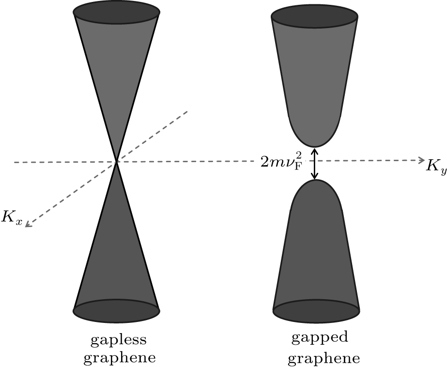 | Fig. 1. Energy spectra of quasiparticles in (a) gapless and (b) gapped graphene. |
In this paper, we consider clean gapped graphene-based ferromagnetic/normal/ferromagnetic (FG/NG/FG) junctions where the graphene is fabricated on the SiC and BN substrates separately. The ferromagnetic state can be induced by depositing a ferromagnetic insulator on top of graphene.[43] The magnitudes of the graphene energy gap 
Our model is composed of two similar ferromagnetic layers separated by a normal graphene of thickness L (Fig. 2). Direction of the magnetization of the left ferromagnet is fixed to be upward but the right ferromagnet has magnetization parallel (up) or antiparallel (down) to the magnetization direction of the left ferromagnet. The system is considered to be in the xy-plane. Since the considered graphene nanoribbon is short and wide (i.e., W/L ≫ 1, where L is the thickness of the normal graphene region and W is the width of the graphene sheet), microscopic details of edge and chirality are both neglected.[44, 45]
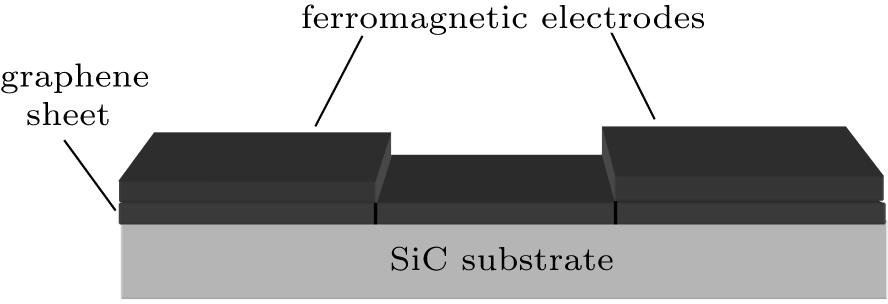 | Fig. 2. Schematic illustration of a gapped FG/NG/FG junction. |
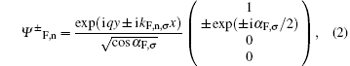
The wave functions describing the quasiparticles are the solutions of the massive Dirac– Bogoliubov– de Gennes equation defined as

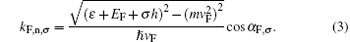
where H0 = − iℏ vF(σ x∂ x ± σ y∂ y) − EFN, with σ x, σ y, and σ z being 2 × 2 Pauli matrices; ε σ is the energy of quasiparticles related to the Fermi level; EFN is the Fermi energy of normal graphene; h is the magnetization exchange energy; vF denotes the Fermi velocity of quasiparticles; σ = ± 1 for up and down spins of quasiparticles; 

While for the normal graphene region
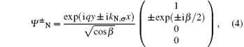
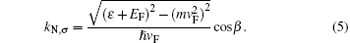
Here kF, n, σ and kN, σ are the components of electron-like wave vector perpendicular to the interface in ferromagnetic and normal graphene regions, respectively. In our calculations, we have 
The refection coefficient r and the transmission coefficient t are calculated by applying the boundary conditions at the interface between ferromagnetic and normal regions. The interfaces between ferromagnets and normal graphene are perpendicular to the x axis at x = 0 and x = L, that is

for x = 0, and

for x = L. Using the boundary conditions (6) and (7), the transmission coefficient for the antiparallel case is obtained as follows:

For the parallel case we only need to set α F, σ = α 1, σ .
Using the approach of Refs. [46]– [48], the differential electronic conductance at zero temperature is

For differential spin conductance at zero temperature, we have
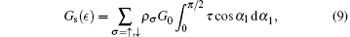
where G0 = 2e2/hNσ (ϵ V) is spin-dependent normal conductance, ρ σ = + 1 (− 1) for σ = ↑ (↓ ), and the density of states is 
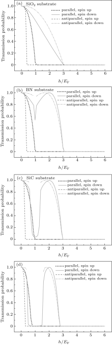
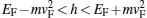
Figure 3 demonstrates the transmission probability (τ = | t| 2) of quasiparticles in terms of the exchange energy of ferromagnets in parallel and antiparallel structures for a gapless case and three gapped cases.
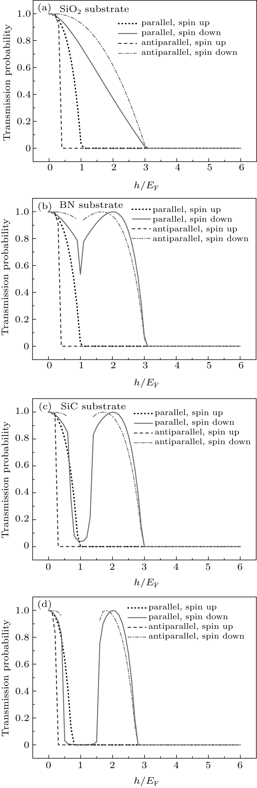 | Fig. 3. Transmission probabilities of electrons versus h/EF of ferromagnets, here, the thickness of the graphene-based normal region is kL= 10. (a) Gapless graphene, (b) gapped graphene fabricated on BN substrate,    |
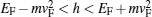
It is observed that for h/EF > 3 the transmission probability is zero for all cases. Also there is an energy interval around the Fermi energy with a size of graphene gap of 

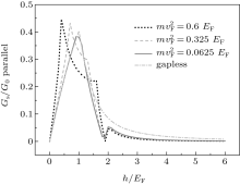
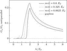
Figures 4 and 5 show the charge conductances of parallel and antiparallel structures versus h/EF of ferromagnets, respectively.
 | Fig. 4. Normalized charge conductances of parallel structure versus h/EF of ferromagnets. Here, the thickness of the graphene-based normal region is kL= 10. |
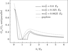
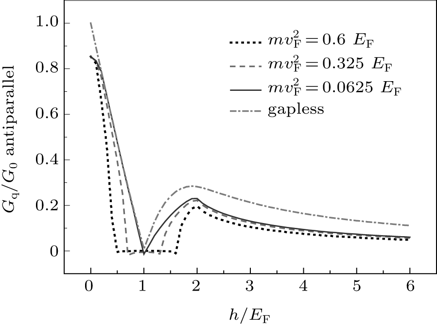 | Fig. 5. Normalized charge conductances of antiparallel structure versus h/EF of ferromagnets. Here, the thickness of graphene-based normal region is kL= 10. |
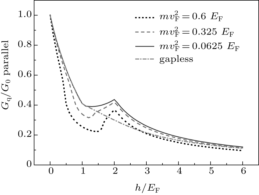
Increasing the strength of ferromagnet h, the potential well will be deeper and charge transport suppresses. It can be seen that the conductance diagrams of gapped parallel structures in terms of the exchange-energy have a special behavior at the energies close to 2EF. For the antiparallel structures, the special behavior at energy close to EF can be seen for both gapless and gapped structures. Also in the range of 
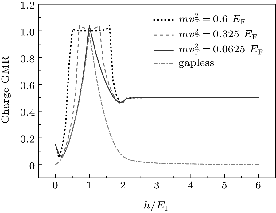 | Fig. 6. Charge GMRs versus h/EF of ferromagnets. Here, the thickness of graphene-based normal region is kL= 10 . |
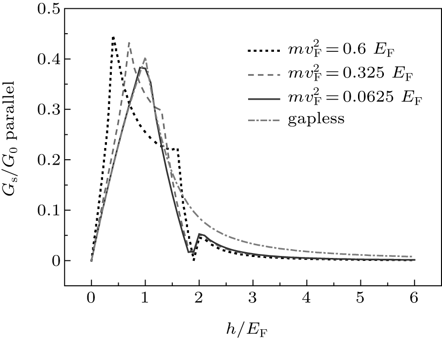
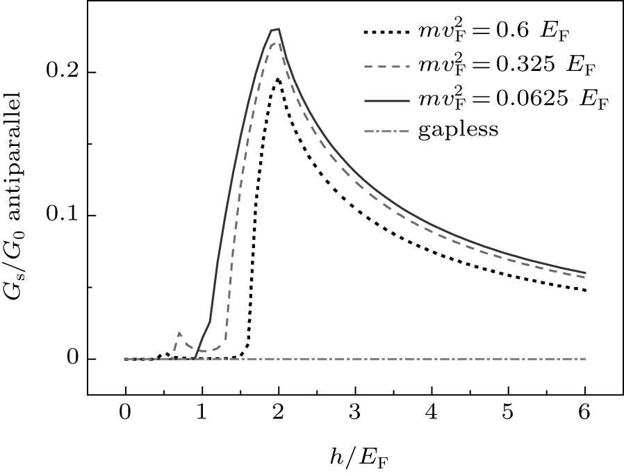
Figures 7 and 8 show spin conductances of parallel and antiparallel structures versus h/EF of ferromagnets. The spin conductance of the gapped parallel structure has different behaviors in energies less than 


 | Fig. 7. Normalized spin conductances of parallel structure versus h/EF of ferromagnets. Here, the thickness of the graphene-based normal region is kL= 10. |
 | Fig. 8. Normalized spin conductances of antiparallel structure versus h/EF of ferromagnets. Here, the thickness of the graphene-based normal region is kL= 10. |
Unlike the parallel structure case, the only effect of increasing the graphene energy gap is to reduce the spin conductance of the antiparallel structure, which has significant magnitude in energy around h ∼ 2EF.
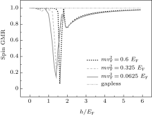
Since parallel and antiparallel spin conductances have significant values in different ranges of energies (except EF < h < 2EF), the spin GMR is almost 1 in most exchange energies as illustrated in Fig. 9.
 | Fig. 9. Spin GMRs versus h/EF of ferromagnets. |
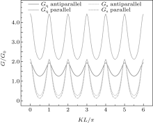
Our calculations show oscillating dependences of transmission probability, charge, and spin conductance on the thickness of the normal graphene region for all exchange energies except 
 | Fig. 10. Transmission probabilities of electrons versus thickness of the normal region, h = 4EF. |
 | Fig. 11. Charge and spin conductance of electrons versus thickness of the normal region, h = 4EF. |
We studied the electronic and spintronic conductances in parallel and antiparallel clean gapped graphene-based FG/NG/FG junctions by taking into account the effect of the exchange energy of magnetic layers and thickness of the normal graphene region.
In our calculations, the experimental data given in Refs. [6], [10], and [11] are used. For gapped graphene grown on SiC and BN substrates, the values of energy gap 
It is illustrated that despite gapless FG/NG/FG structures, which can be used to acquire spin-up (or spin-down) polarized current (see Ref. [16]), the gapped FG/NG/FG structures can be used for both spin-up and spin-down polarized currents. It means that they can be used as a spin-polarized current switch. Also in the gapped FG/NG/FG structure, perfect charge GMR is observed in the range of 
| 1 |
|
| 2 |
|
| 3 |
|
| 4 |
|
| 5 |
|
| 6 |
|
| 7 |
|
| 8 |
|
| 9 |
|
| 10 |
|
| 11 |
|
| 12 |
|
| 13 |
|
| 14 |
|
| 15 |
|
| 16 |
|
| 17 |
|
| 18 |
|
| 19 |
|
| 20 |
|
| 21 |
|
| 22 |
|
| 23 |
|
| 24 |
|
| 25 |
|
| 26 |
|
| 27 |
|
| 28 |
|
| 29 |
|
| 30 |
|
| 31 |
|
| 32 |
|
| 33 |
|
| 34 |
|
| 35 |
|
| 36 |
|
| 37 |
|
| 38 |
|
| 39 |
|
| 40 |
|
| 41 |
|
| 42 |
|
| 43 |
|
| 44 |
|
| 45 |
|
| 46 |
|
| 47 |
|
| 48 |
|
| 49 |
|
| 50 |
|
| 51 |
|
| 52 |
|