An ultra-low specific on-resistance trench LDMOS with a U-shaped gate and accumulation layer

An ultra-low specific on-resistance trench LDMOS with a U-shaped gate and accumulation layer |
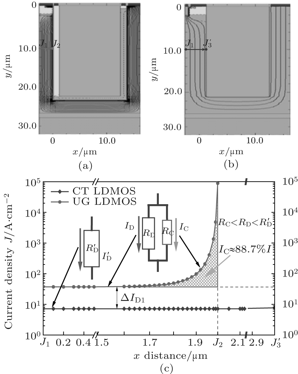
| Flow line distributions of (a) UG LDMOS (12.4 mΩ·cm2) and (b) CT LDMOS (346.6 mΩ·cm2) (5 × 10⁻⁸ A·μm−1/contour) with the optimal doping concentration of the drift region. (c) Current density distributions under the source ( y = 10.0 μm). |
 |