


Novel attributes and design considerations of effective oxide thickness in nano DG MOSFETs
[Charmi Morteza† ]
]
]
|
|


†Corresponding author. E-mail: charmi@guilan.ac.ir
Impacts of effective oxide thickness on a symmetric double-gate MOSFET with 9-nm gate length are studied, using full quantum simulation. The simulations are based on a self-consistent solution of the two-dimensional (2D) Poisson equation and the Schrödinger equation within the non-equilibrium Green’s function formalism. Oxide thickness and gate dielectric are investigated in terms of drain current, on-off current ratio, off current, sub-threshold swing, drain induced barrier lowering, transconductance, drain conductance, and voltage. Simulation results illustrate that we can improve the device performance by proper selection of the effective oxide thickness.
In order to scale complementary metal– oxide semiconductor (CMOS) devices to nano-scale dimensions while maintaining good control of the short-channel effects and good sub-threshold behavior, not only the physical length and width, but also the gate oxide thickness of metal– oxide semiconductor field-effect transistor (MOSFET) devices must be reduced in approximate proportions.[1] The continued scaling of SiO2 gate oxide is becoming very challenging since a large direct tunneling current flows between the gate electrode and the silicon substrate, which increases standby power consumption and diminishes device performance.[2– 4] Therefore, it has become necessary to use high-k gate dielectrics in order to meet the stringent requirements on gate leakage current and equivalent oxide thickness (EOT).[5– 7] However, use of a high-k gate material (ZrO2, [8] Al2O3, [9] HfO2, [10] etc.) with a fixed equivalent oxide thickness (EOT) causes an increase in the dielectric thickness, resulting in increased fringing fields from the gate to the source/drain regions or Fringing Induced Barrier Lowering (FIBL)[11, 12] and compromised short-channel performance. Of course there are many ways to reduce the FIBL effect and improve the device performance.[13, 14]
In this paper we study an ultra-thin body DG MOSFET with different effective oxide thicknesses (EOT) by consideration of variable oxide thickness (Tox) at fixed dielectric permittivity (k), and variable k at fixed Tox. The simulation is based on a self-consistent solution of the 2D Poisson equation and the Schrö dinger equation, within the non-equilibrium Green’ s function (NEGF) formalism. The effects of EOT on device performance are investigated, namely drain current, on-off current ratio, off current, sub-threshold swing, drain-induced barrier lowering, transconductance, drain conductance, and voltage gain.
Figure 1 is a schematic diagram of the symmetric DG MOSFETs and the corresponding coordinates, where the x axis is along the channel (transport direction), the z axis is along the quantum confinement direction and the y-dimension is treated as infinite. However, quantum confinement in the z direction introduces subbands, and for an ultra thin body, only a few subbands are occupied. A short-channel length (LG = 9 nm), ultra-thin channel, moderate body doping and highly doped source/drain (S/D) contact have been considered. We use abrupt junctions and no S/D doping gradient, to provide a clear answer to the effects of the source/drain capacitor. The parameters of EOT: oxide thickness (Tox) and gate dielectric permittivity (k), are variable. The structural parameters of the devices are presented in Table 1.
| Table 1. Parameters for the DG MOSFET structure used in simulation. |
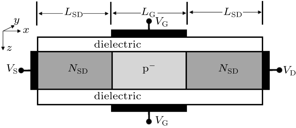 | Fig. 1. An ultra-thin body DG MOSFET structure. |
The 2D ballistic transport equation in the MOSFET channel region was solved by a mode space approach, [15] which splits the problem into two one-dimensional (1D) problems. In the quantum confinement direction (the z direction), the Schrö dinger equation was solved to generate the subbands. In the transport direction (the x direction), the non-equilibrium Green’ s function approach which is equivalent to solving the Schrö dinger equation with the open boundary condition, was used to describe the ballistic quantum transport.
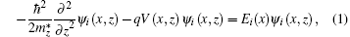
In the vertical direction (z direction in Fig. 1), the Schrö dinger equation was solved for each x-position independently to generate the i-th subband profile, Ei(x), and the corresponding wave function, ψ i(x, z):
where 
For the subband i, with a planewave eigenenergy 
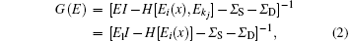
where Σ S and Σ D are the self-energies of the source and drain, respectively, 

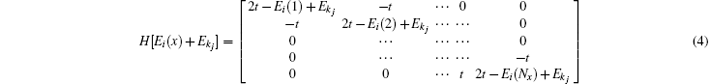
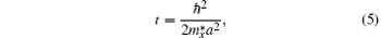
is the Hamiltonian for subband i, with a planewave eigenenergy
where 

where 
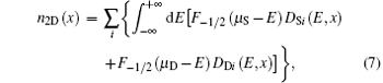
where F− 1/2 is the Fermi integral of order − 1/2, [19]μ S (μ D) is the source/drain Fermi level, and DSi (E, x) (DDi (E, x)) is the local density of states (LDOS) of the i-th subband contributed by the source (drain), which is calculated based on Green’ s function formalism. The 2D electron density, n2D (x), is then weighted by the eigenfunction at the position x, ψ i (x, z), to get the 3D electron density:

A 2D Poisson equation was then solved for the silicon channel and gate oxide to update the electrostatic potential. (A nonlinear Poisson equation was solved to improve the outer loop convergence.[20]) The iteration between the quantum transport equation and the Poisson equation was repeated until self-consistency was achieved. Finally we can calculate the source– drain current:[16]
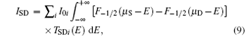
where I0i is a constant with the dimension of current, F− 1 / 2 is the Fermi– Dirac integral of order − 1/2, μ S/D is the source/drain Fermi level, i indexes the subbands and TSDi is the transmission coefficient from the source to drain for the i-th subband at energy E

The equivalent oxide thickness (EOT) is defined as[21]

where khigh-k and thigh-k are the dielectric constant of high-k material and physical thickness of high-k dielectric film, respectively, and 3.9 is the dielectric constant of silicon oxide. According to the above equation, for investigation of EOT, we need to study the properties and impacts of khigh-k and thigh-k on the performance of DG-MOSFETs. According to the end of the international technology roadmap for semiconductors (ITRS) 2012, [22] the Ioff (VGS = 0 V and VDS = 0.6 V) is equal to 0.1 μ A/μ m and EOT = 0.5 nm. To produce EOT = 0.5 nm, we use khigh-k = 15 and thigh-k = 1.93 nm, and to produce Ioff = 0.1 μ A/μ m, we use the gate work function, ϕ = 4.370 eV. This value of the gate work function is a fixed parameter in all overdrives in this article. Moreover, for study of short channel MOSFTEs, it is necessary to apply the 2D electrostatics and the capacitor model for 2D electrostatics. The MOSFET’ s gate electrode induces a charge in the channel of the transistor, but the source and drain electrodes can also induce charge.
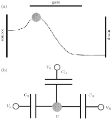
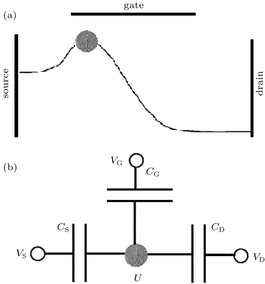 | Fig. 2. Illustration of the capacitor model of 2D electrostatics, (a) the conduction band profile under high gate and drain bias with the inversion layer charge at the top of the barrier identified, (b) a three-capacitor model that describes the control of the potential at the top of the barrier. |
As sketched in Fig. 2(a), our interest is in the potential and charge at the top of the barrier. The three-capacitor model of Fig. 2(b) describes the modulation of the potential and charge at the top of the barrier by the three terminals. This simple model provides an alternative, and very physical, picture of 2D MOSFET electrostatics. In the three-capacitor model, the charge (Q) and potential (U) at the top of the barrier are related by

where CG, CD, CS, and CT are the gate capacitor, drain capacitor, source capacitor, and total capacitor, respectively. The gate capacitance is the series combination of the oxide capacitance and the semiconductor capacitance, also in ultra-thin MOSFET CG ≈ Cox for above threshold operation.[18] The quantum capacitance is not shown explicitly but is implicit in the treatment of band filling and is included naturally through the treatment of self-consistent gate electrostatics. In this work, we first investigate the effect of oxide thickness, and then the impact of high-k gate dielectric is studied.
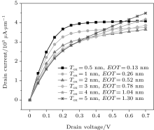
In this section, the oxide thickness and EOT are varied while the high-k gate dielectric permittivity is fixed at 15. Figure 3 shows the drain current versus drain voltage for different oxide thicknesses and different EOT, at VG = 0.6 V. It is clear that for a small oxide thickness (less than 2 nm) the drain current is saturated at high drain voltage, while for a large oxide thickness (larger than 2 nm) the drain current is increased with increasing drain voltage. Because a smaller Tox gives a higher oxide capacitor (Cox) and a higher CG, which ultimately lead to an increase in the ratio of the gate capacitance (CG) to total capacitance (CT). Therefore, the control of the gate on the channel is increased, the device acts like a long channel transistor and the drain current is saturated at high drain voltage. While, for larger Tox values, the CG is decreased, the ratio of the drain capacitance (CD) to total capacitance (CT) is increased and the control of the drain on the channel is increased. So the device acts like a short channel transistor and the drain current is increased with increasing drain voltage.
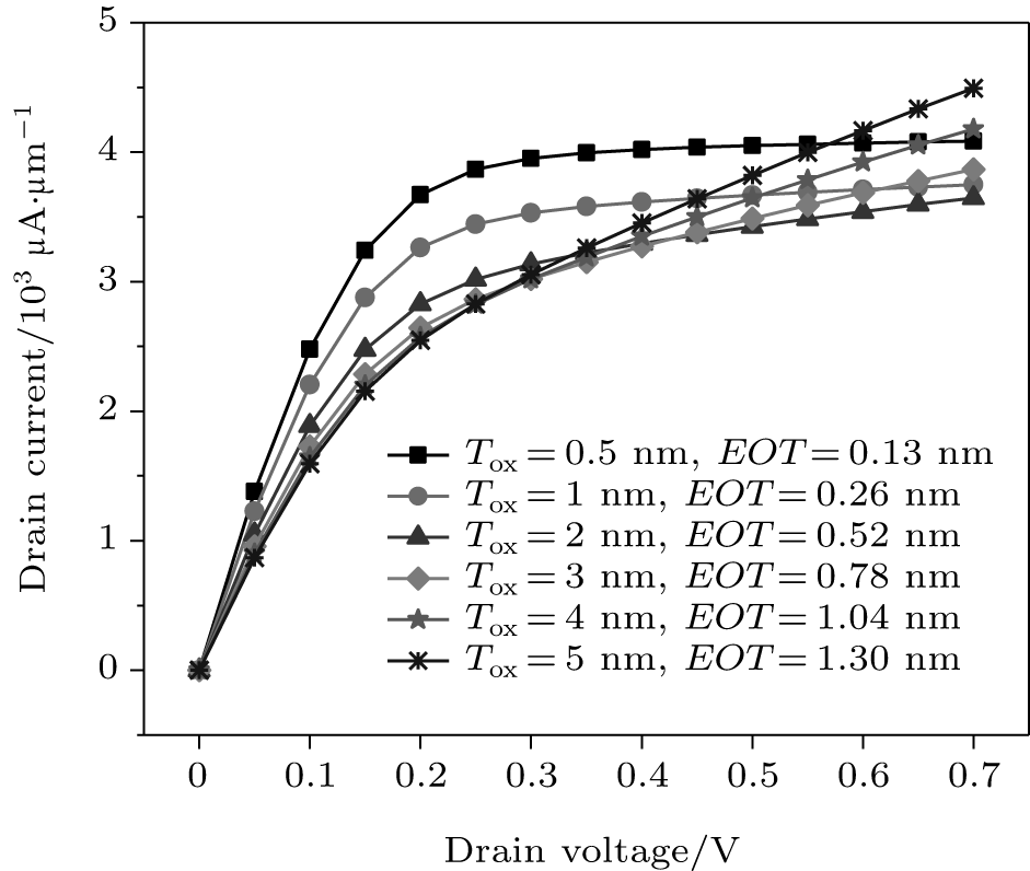 | Fig. 3. Drain current versus drain voltage for different oxide thicknesses and different EOT, at VG = 0.6 V. |
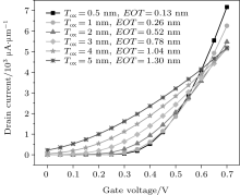
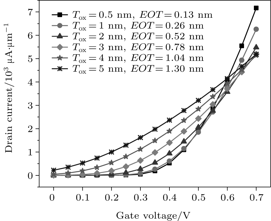
Figure 4 shows the drain current versus gate voltage for different oxide thicknesses and different EOTs, at VD = 0.6 V. It is readily apparent that by incrementing Tox and EOT, the threshold voltage is decreased. Moreover, at lower gate voltage, due to the low threshold voltage and high off current, by increasing the Tox and EOT, the current is increased. While at higher gate voltage, due to an increase of both accumulated charge and Cox, by decreasing Tox the current is increased.
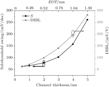
It is worth noting that, from Figs. 5– 7, we have two horizontal axes, and the lower axis shows the oxide thickness (Tox = 0.5 nm– 5 nm) and the upper axis shows the effective oxide thickness (EOT = 0.13 nm– 1.30 nm).
 | Fig. 4. Drain current versus gate voltage for different oxide thicknesses and different EOT, at VD = 0.6 V. |
 | Fig. 5. (a) Off current and (b) on– off current ratio versus oxide thickness (lower axis) and EOT (upper axis). |
When we use a fixed gate work function in MOSFETs, due to varying the off-current, the on-current to off-current ratio (Ion/Ioff) becomes a more important parameter than the on-state current (VD = 0.6 V and VG = 0.6 V). The off-current (VD = 0.6 V, VG = 0 V) and Ion/Ioff versus Tox and EOT are shown in Fig. 5(a) and Fig. 5(b), respectively. At off-state (VG = 0 V, VD = 0.6 V), with increasing Tox and EOT, the Cox and CG are decreased, the control of the gate on the channel is decreased and CD/CT is increased, so the source-to-drain tunneling current is increased, which leads to increased off-current. Also, as can be seen from Fig. 5(b), with increasing Tox and EOT, due to the increase of the off-current, the Ion/Ioff is decreased. In addition, the on– off current ratio, in its maximum value, is almost 172, 244 times its minimum value, although the minimum Tox is 0.5 nm and the maximum Tox is 5 nm. Therefore, the oxide thickness has an important impact on the performance of DG MOSFEs that must be considered. It is important that we are not considering the series resistance and scattering processing in our simulation. Therefore, the drain current in our DG MOSFET is certainly greater than the experimental data of a respective device.
For a well-designed MOSFET, the subthreshold swing (S) is less than 80 mV/decade, and the drain-induced barrier-lowering (DIBL) is less than 100 mV/V.[18] The effective oxide capacitance (Cox) is a key component in determining the short channel effects, since it directly influences how well the channel conductance is controlled by the gate voltage. Thus, it affects the subthreshold swing and DIBL. The subthreshold swing and DIBL are increased with increasing Tox and EOT, as is shown in Fig. 6. With increasing Tox and EOT, the Cox and CG are decreased, the control of the gate on the channel is decreased, so the leakage current, source-to-drain tunneling current, and off-current are increased, which lead to an increase of the subthreshold swing. Also, the barrier height for channel carriers at the edge of the source is reduced, due to the influence of the drain electric field upon the application of drain voltage. This increases the number of carriers injected into the channel from the source, leading to increased drain off-current and shows drain-induced barrier-lowering for devices with increasing Tox and EOT, and it increases the DIBL effect. For our nominal device (Table 1) and according to Fig. 6, we can use a Tox only up to 2 nm, greater values of Tox give an S parameter bigger than 80 mV/dec and a DIBL bigger than 100 mV/V, which are not suitable for a well-designed MOSFET.
The dependence of transconductance (gm), drain conductance (gd), and voltage gain (gm/gd) upon oxide thickness at on-state, VD = VG = 0.6 V, are shown in Fig. 7(a), 7(b), and 7(c), respectively. The minimum value of Tox is the best value for transconductance, drain conductance and voltage gain. Transconductance is the ratio of the drain current variation to the gate voltage variation. Therefore in the on-state, according to Fig. 4, with increasing Tox, this gradient decreases and gm decreases (Fig. 7(a)). Drain conductance is the ratio of the drain current variation to the drain voltage variation. According to Fig. 3, in the on-state, increasing Tox increases both this gradient and gd (Fig. 7(b)). Also the voltage gain decreases with increasing Tox (Fig. 7(c)).
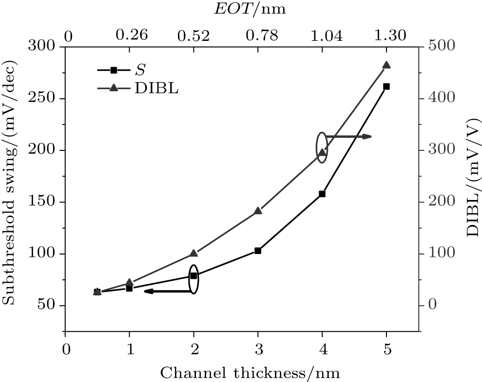 | Fig. 6. Subthreshold swing and DIBL versus oxide thickness (lower axis) and EOT (upper axis). |
 | Fig. 7. (a) Transconductance, gm, (b) drain conductance, gd, and (c) voltage gain, gm/gd versus oxide thickness (lower axis) and EOT (upper axis), at VD = VG = 0.6 V. |
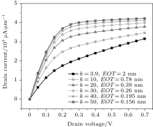
In this section, the oxide dielectric permittivity (k) and EOT are varied while the oxide thickness is fixed at 2 nm. Figure 8 shows the drain current versus drain voltage for different dielectric permittivity values and different EOT, at VG = 0.6 V. It is clear that at high drain voltage, for higher k gate, the drain current is saturated, while for lower k, the drain current is increased with an increase of the drain voltage. For higher k, the Cox and CG are increased, the ratio of the gate capacitance (CG) to total capacitance (CT) is increased and the control of the gate on the channel is increased, so the drain current is saturated at high drain voltage. For lower k (higher EOT), the CG is decreased, the ratio of the drain capacitance (CD) to total capacitance (CT) is increased and the control of the drain on the channel is increased. So the device acts like a short channel transistor and the drain current increases with increasing drain voltage. Moreover, by incrementing k, due to an increase of the oxide capacitor, the drain current is increased.
 | Fig. 8. Drain current versus drain voltage for different gate dielectric permittivities and different EOTs, at VG = 0.6 V. |
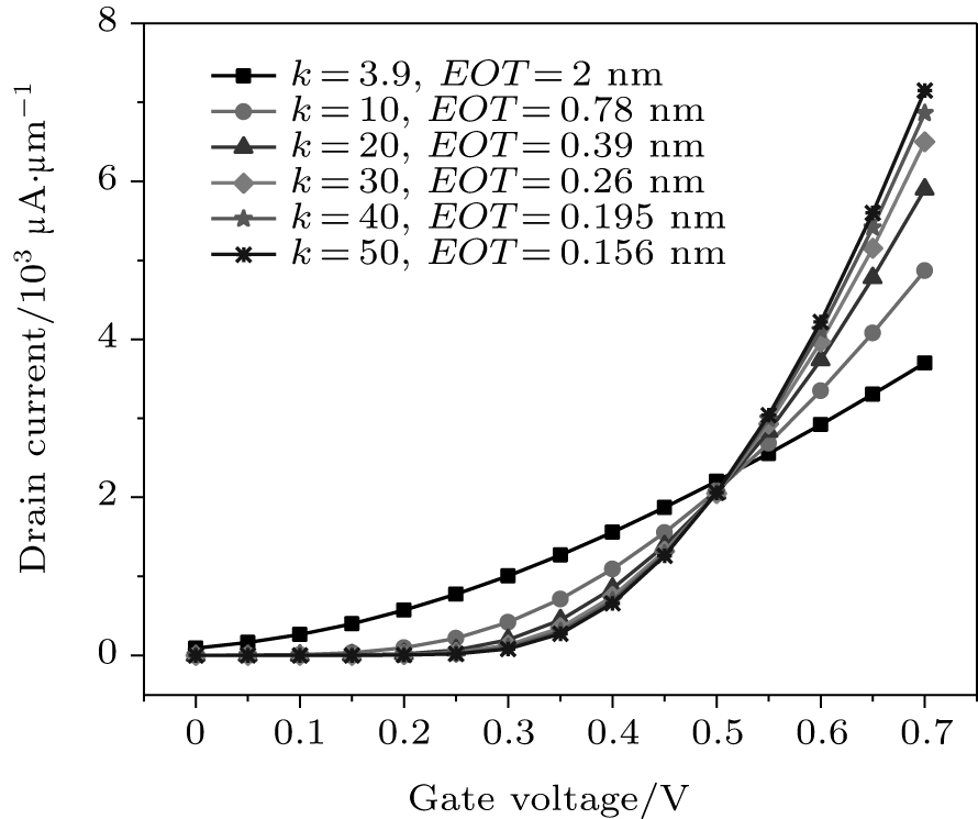
Figure 9 shows the drain current versus gate voltage for different dielectric (k) and EOT, at VD = 0.6 V. It is evident from Fig. 9 that by increasing k and decreasing EOT, the threshold voltage is increased. At lower gate voltage, due to high threshold voltage and low off current, by increasing k and decreasing EOT, the drain current is decreased. While at higher gate voltage, due to an increase of accumulated charges, Cox and CG, the drain current is increased with an increment of k.
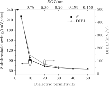
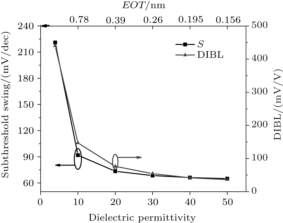
Note that, from Fig. 10 to Fig. 12, we have two horizontal axes: the lower axis shows the gate dielectric permittivity (k = 3.9 nm– 50 nm), and the upper axis shows the effective oxide thickness (EOT = 0.156 nm– 2 nm), and its direction is opposite that of the lower axis. The off-current and Ion/Ioff versus k and EOT are shown in Figs. 10(a) and 10(b), respectively. With increasing k and decreasing EOT, Cox and CG increase and CD/CT decreases. So the source-to-drain tunneling current is decreased, which leads to decreased off-current and increased Ion/Ioff. In addition, the on-off current ratio at its maximum value is almost 37871 times its minimum value.
 | Fig. 9. Drain current versus gate voltage for different gate dielectric permittivities and different EOTs, at VD = 0.6 V. |
 | Fig. 10. (a) Off current and (b) on– off current ratio versus gate dielectric permittivity (lower axis) and EOT (upper axis). |
Figure 11 illustrates the subthreshold swing and DIBL versus gate dielectric permittivity and EOT. It is readily apparent that the subthreshold swing and DIBL decrease with increasing k and decreasing EOT, as already discussed with regard to Fig. 6. For a well-designed MOSFET and according to Table 1, we can use a gate dielectric permittivity only above 15. The dependence of gm, gd, and gm/gd versus k and EOT at on-state, are shown in Fig. 12(a), 12(b), and 12(c), respectively. As discussed with regard to Fig. 7, at on-state, with increasing k, gm is increased, gd decreases and the voltage gain increases, as shown in Fig. 12.
 | Fig. 11. Subthreshold swing and DIBL versus gate dielectric permittivity (lower axis) and EOT (upper axis). |
 | Fig. 12. (a) Transconductance, gm, (b) drain conductance, gd, and (c) voltage gain, gm/gd versus gate dielectric permittivity (lower axis) and EOT (upper axis), at VD = VG = 0.6 V. |
A self-consistent solution of the NEGF and Poisson equations has been used in order to investigate the impacts of oxide thickness and gate dielectric permittivity on the ultra-thin double gate MOSFETs. For our conceptual device, it is found that the output characteristics are more sensitive to the oxide thickness than to the gate dielectric permittivity. In this way, we could also find proper oxide thickness and gate dielectric permittivity parameters for improving the performance of nanoscale double gate MOSFETs.
| 1 |
|
| 2 |
|
| 3 |
|
| 4 |
|
| 5 |
|
| 6 |
|
| 7 |
|
| 8 |
|
| 9 |
|
| 10 |
|
| 11 |
|
| 12 |
|
| 13 |
|
| 14 |
|
| 15 |
|
| 16 |
|
| 17 |
|
| 18 |
|
| 19 |
|
| 20 |
|
| 21 |
|
| 22 |
|