


Boron implanted emitter for n-type silicon solar cell*
[Liang Peng† , Han Pei-De, Fan Yu-Jie, Xing Yu-Peng]
, Han Pei-De, Fan Yu-Jie, Xing Yu-Peng]
|
|


†Corresponding author. E-mail: liangpeng@semi.ac.cn
*Project supported by the National Natural Science Foundation of China (Grant Nos. 61275040, 60976046, and 61021003) and the National Basic Research Program of China (Grant No. 2012CB934200).
The effects of ion doses on the properties of boron implanted Si for n-type solar cell application were investigated with doses ranging from 5× 1014 cm− 2 to 2× 1015 cm− 2 and a subsequent two-step annealing process in a tube furnace. With the help of the TCAD process simulation tool, knowledge on diffusion kinetics of dopants and damage evolution was obtained by fitting SIMS measured boron profiles. Due to insufficient elimination of the residual damage, the implanted emitter was found to have a higher saturation current density ( J0e) and a poorer crystallographic quality. Consistent with this observation, Voc, Jsc, and the efficiency of the all-implanted p+–n–n+ solar cells followed a decreasing trend with an increase of the implantation dose. The obtained maximum efficiency was 19.59% at a low dose of 5× 1014 cm− 2. The main efficiency loss under high doses came not only from increased recombination of carriers in the space charge region revealed by double-diode parameters of dark I– V curves, but also from the degraded minority carrier diffusion length in the emitter and base evidenced by IQE data. These experimental results indicated that clusters and dislocation loops had appeared at high implantation doses, which acted as effective recombination centers for photogenerated carriers.
The design and fabrication of a high quality emitter is of paramount importance to realize high efficiency solar cells. The state of the art doping technique using ion implantation has gained increasing interest in the solar cell community, as it is an alternative way to the traditional tube furnace diffusion process for forming the pn junction. As far back as 1980, Douglas and co-workers had determined experimentally the factors that control the solar cell efficiency by a systematic variation of the ion-implantation parameters and the post annealing conditions.[1] It was later revealed that an open circuit voltage as high as 0.645 V (AM0) could be obtained by adopting the phosphorus implantation technique on low resistivity boron-doped starting materials.[2] Notably in 1984, an ion-implanted silicon solar cell with the highest AM1 efficiency of 18% was reported, which comprised an all implanted n+ – p– p+ structure.[3] The preceding results unambiguously establish that the ion implantation technique is suitable for high efficiency solar cell production even though high cost and low yield limit its further development. Very recently, the ion-implanter specially tailored for PV applications becomes commercially available[4] and has been used to fabricate solar cells with very low saturation current densities and high efficiencies above 20%.[5] A novel selective doping approach using in situ masking makes it compelling that the patterned ion implantation might be a preferable way to realize the SE architecture.[6] Besides, the more economically acceptable doping technique called plasma immersion ion implantation (PIII) is finding its place in the solar cell market because of its simple and robust structure and ability to implant a high dose in a large substrate in a short time.[7]
In view of the benefits of utilizing n-type silicon as the starting wafer for solar cell production, [8] most advanced high efficiency n-type solar cells feature a diffused emitter in the homogeneous front junction or interdigitated back junction pattern. Taking the prominent advantages of the ion implantation process into consideration, [4] there is a need to investigate the high quality ion-implanted boron emitter for n-type solar cell application. However, as the high energy ion bombardment induced damage is inevitable, how to eliminate those defects and activate the dopants to the maximum deserves our attentive study to achieve the optimum solar cell efficiency. Another formidable problem associated with the boron doped emitter is the poor passivating quality of the traditional dielectric films such as SiO2 and SiNx.[9] Al2O3 is viewed as an appropriate alternative because of its inherent high concentration of negative charges, and its application in solar cells has been intensively studied.[10]
In this paper, we study the effects of the implantation dose on the performance of solar cells. Emphasis is given to the experimental optimization of the emitter doping profile. A physical interpretation of the dopant dose dependent efficiency is also given. In Section 2, we present the experimental details of solar cell fabrication. Electrical and crystallographic material characterizations of the boron doped emitter are conducted in Section 3. In Section 4, through performance analysis of all-implanted p+ -n-n+ silicon solar cells, the impact of the implantation dose on the solar cells is pointed out at the device level. Finally in Section 5, we draw the conclusions from the present study.
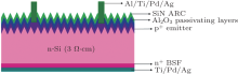
N-type CZ wafers with a resistivity of 3 Ω · cm and thickness of 380 μ m received a first thermal oxidation and a subsequent “ inverted pyramid” texturing of the top surface. A P-type emitter was formed by boron ion implantation through lithographically defined 2 cm× 2 cm isolation windows with a constant acceleration energy of 32 keV and variable doses of 5× 1014 cm-2 to 2× 1015 cm-2. The implantation beam current was maintained to be less than 100 μ A. The wafer surface was offset by 7° from the beamline to avoid ion channeling. Next the phosphorus ions were implanted into the back surface to form BSF with a dose of 3× 1015 cm-2, yielding a sheet resistance of about 20 Ω /⧉ after annealing. All implants were done at room temperature using a research type medium energy ion implanter with a mass-analyzer. After careful RCA cleaning, the implanted wafers were then annealed in the conventional tube furnace with two successive steps. They were at first annealed at 560 ° C for 90 min in dry N2. After the temperature ramped up to 1000 ° C, they subsequently received an in situ high temperature annealing for another 30 min to obtain good activation of the dopants. The first long time low temperature isochronal annealing step was believed to be essentially important for implantation damage removal, according to the previous studies, [11, 12] and has been applied to fabricate high efficiency ion-implanted solar cells.[1– 3] Then all the annealed samples were passivated by Al2O3 with a thickness of about 20 nm realized by a thermal atom-layer-deposition system and finally capped with an optimized SiNx anti-reflective layer through plasma enhanced chemical vapor deposition. Front and back metallization was made by evaporation. Contact stripes were designed that were 10 μ m in width to reduce inferior recombination in the metalized areas. As the last step, all the wafers underwent forming gas annealing (@400 ° C, 30 min) and Ag plating with the final grid finger width about 15 μ m and height about 8 μ m. The all-implanted p+ – n– n+ cell structure is schematically presented in Fig. 1.
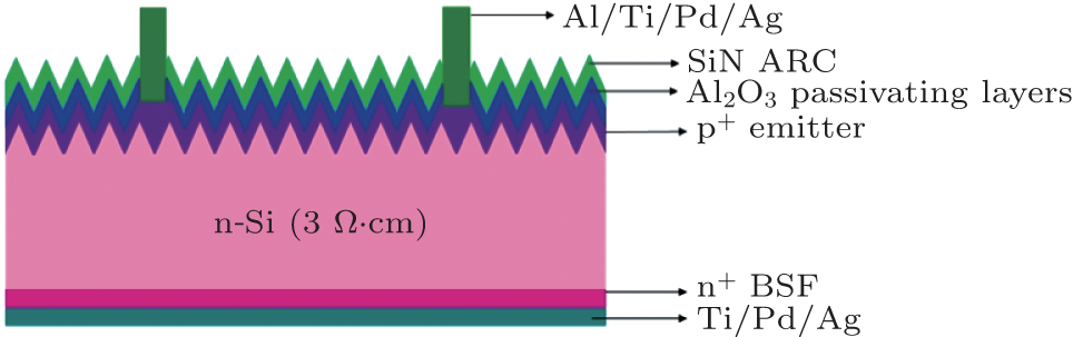 | Fig. 1. Schematic cross section of the front junction solar cell structure. |
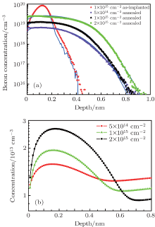
Figure 2(a) demonstrates secondary ion mass spectroscopy (SIMS) measured doping profiles and their respective simulated ones based on the Athena process simulator (TCAD) at various doses. The as-implanted sample is modeled using statistically based Monte Carlo calculation of ion trajectories on the basis of binary collision approximation (BCA). Some main models adopted in the annealing simulation include the full coupled diffusion model allowing for the interaction of dopants and nonequilibrium point defects, the {311} cluster damage model accounting for the evolution of interstitial clusters, and the high concentration model describing the higher-order pairing of defect-dopant/defect.[13] As can be seen from the graph, all doping profiles of the samples are accurately reproduced by the simulation, indicating that the parameters related with the dopant diffusion have been appropriately chosen. Based on these parameters, the profiles of the remnant interstitial cluster concentration for the annealed samples are obtained and displayed in Fig. 2(b). There is an obvious trend that the concentration of the remnant interstitial clusters in the annealed boron implanted samples increases with increasing initial dopant dose.
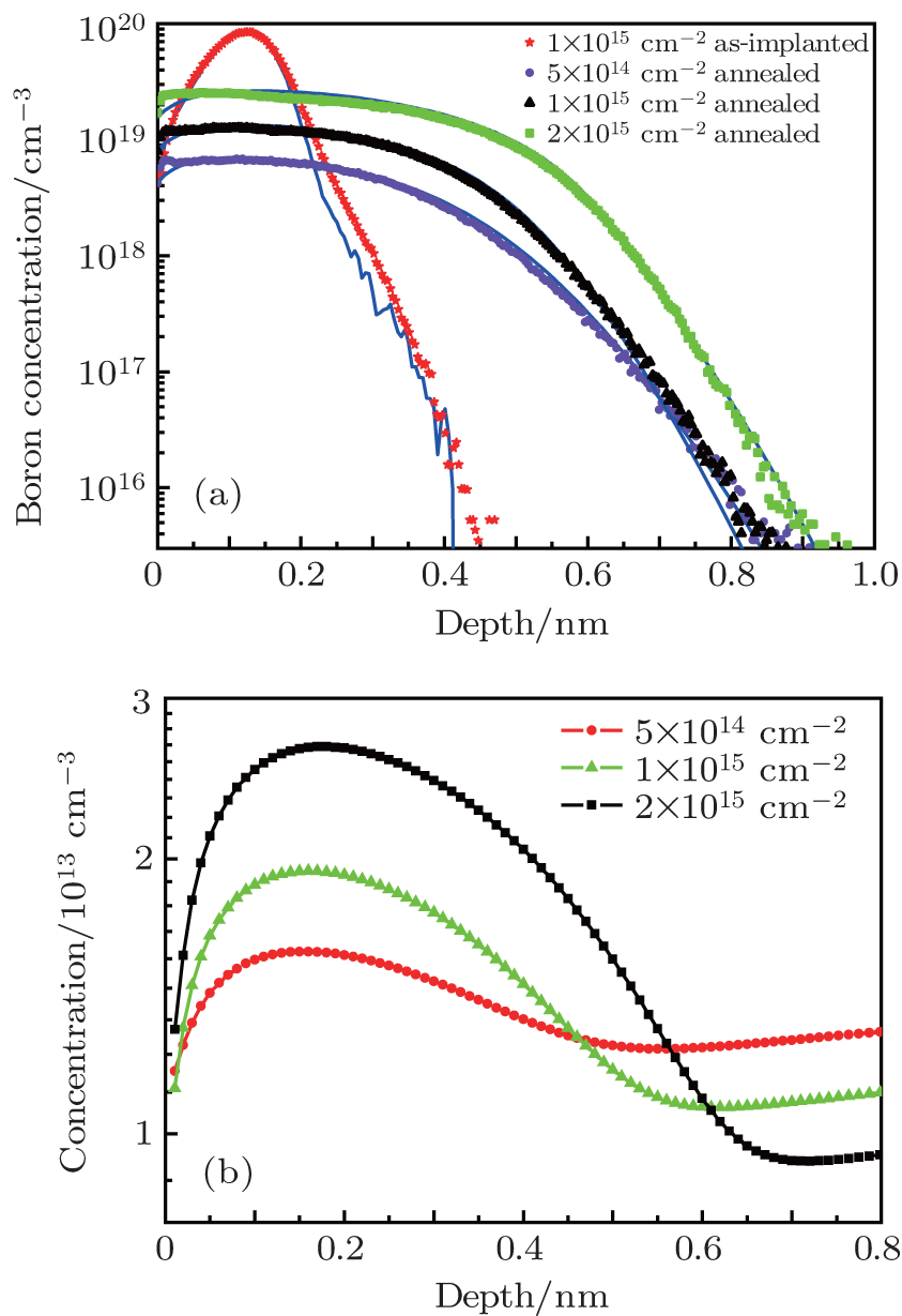 | Fig. 2. (a) SIMS measured (symbols) and TCAD simulated (lines) doping profiles for some typically selected boron implanted samples before and after annealing. (b) TCAD simulated remnant interstitial cluster concentration profiles for the boron annealed samples in panel (a). |
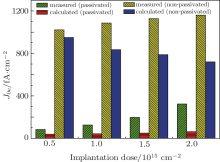
Contactless quasi-steady-state photoconductivity (QSSPC) measurement[14] was performed to evaluate the quality of the emitter. All the samples received bifacial boron implantation with doses, annealing, and passivation identical to those of the fabricated solar cells. Afterwards, the passivation layers were removed and emitter saturation current densities J0e of these non-passivated samples were measured again. In addition, a theoretical calculation of J0e for the passivated and the non-passivated wafers at different doses was performed for comparison with the experimental data based on the emitter boron doping profiles and the surface recombination velocity.[15] The calculated intrinsic limits of J0e together with the measured values for both passivated and non-passivated wafers are displayed in Fig. 3.
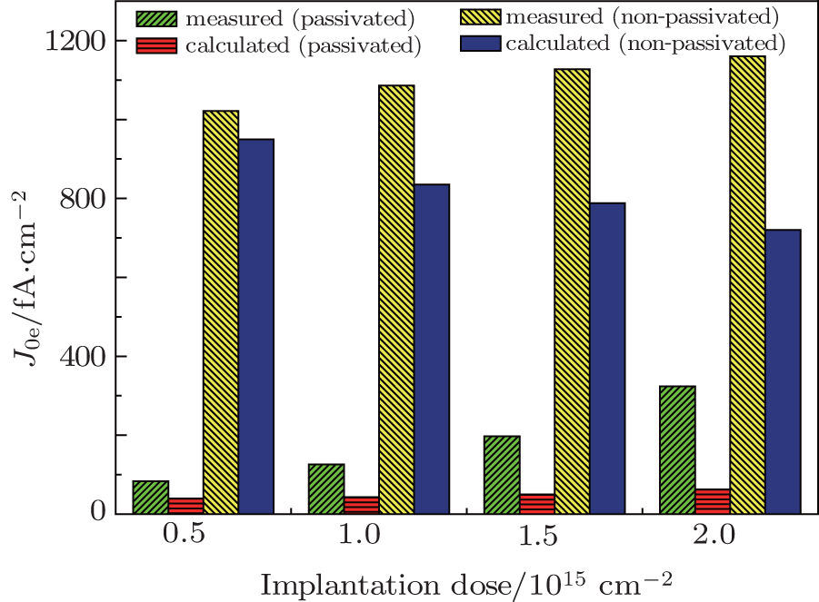 | Fig. 3. Emitter saturation current density J0e obtained by QSSPC measurement and theoretical calculation. |
From the comparison of data in Fig. 3, we can find that the theoretically calculated ideal J0e values for the passivated samples at corresponding doses are 2– 4 times lower than the measured ones. Increasing the implantation dose results in more pronounced degradation of J0e and larger deviation from ideality. Since the implanted region is non-amorphized below the boron dose of 1.5× 1016 cm-2, [16] the concentration of residual damage after annealing increases with increasing implantation dose, just as figure 2(b) reveals. Accordingly, significantly increased bulk SRH recombination in the implanted region is the main cause of increased J0e. Thus, a higher thermal budget is needed to completely remove the residual damage under a heavier implantation dose. After stripping out the passivating layers, the samples show drastically increased J0e values (all above 1000 fA/cm2) and a slight increase with implantation doses (138 fA/cm2). This is mostly likely due to the fact that the added high surface recombination dominates the emitter saturation current density. The defects below the surface of the implanted region have no major impact on J0e, because the injected minority carriers recombine mostly in the surface. The calculated J0e for the non-passivated samples decreases as the dose increases. This is because the high surface concentration induces a stronger “ doping gradient field” , which can repel the minority carriers effectively from the highly recombinative surface, thus leading to an improvement of J0e.[3] The non-passivated sample with a 5× 1014 cm− 2 dose shows a measured J0e very close to calculation. This again implies that no obvious residual damage is left after the present thermal annealing.
The crystallographic characteristics of the above samples were also checked by X-ray diffraction (XRD) analyses. Figure 4 gives the measured rocking curves for these annealed specimens with different implantation doses. The diffraction intensity in the longitudinal axis is normalized to eliminate the effect of incident X-rays on the intensity of diffracted rays. As can be seen, a trend of lower crystallinity with increasing implantation dose is qualitatively consistent with Fig. 3, which reveals a higher J0e with increasing implantation dose. Specifically, the much broader intensity tailing at angles greater than exact Bragg angle θ 0 unambiguously reveals that an extremely disordered crystalline region exists, which has a lattice constant smaller than the intrinsic value d0 according to the Bragg condition (λ = 2dsin θ ). This is in principle consistent with the result in Ref. [17].
 | Fig. 4. Implantation dose dependence of rocking curves. |
According to the literature, [18] a beam of accelerated ions entering the originally perfect crystalline silicon is slowed down or scattered by interacting with the silicon atoms. Along each ion trajectory, fast recoiling atoms create so called Frenkel point defect pairs of vacancy and interstitial. These lattice vacancies and interstitials will annihilate one after another during high temperature annealing, leaving, in principle, one silicon interstitial for each substitional boron atom. Higher doses of boron will result in a higher concentration of silicon interstitials. They have very high diffusivity even at room temperature before being trapped by native defects.[19] At high annealing temperature, this significant amount of excessive interstitials can migrate quickly, superpose and gather to create secondary defects called clusters. These clusters can evolve from small ones to bigger ones and finally to extended defects called dislocation loops if the initial damage exceeds a limit, one that we call the threshold damage. Transmission electron microscopy and simulation studies[20– 22] show that rod-like clusters lying on {311} planes or stable boron-interstitial clusters in B3 I configuration usually form after 950 ° C annealing for a boron implantation dose higher than 1× 1015 cm− 2. Furthermore, once the dose exceeds 2× 1015 cm− 2, these clusters will form more severe extended defects called end-of-range (EOR) dislocation loops that are stable even at temperatures above 1000 ° C.[21] Structurally, these complex clusters destroy the lattice locally, causing distortions of an otherwise crystalline lattice. Electrically, these recombination centers exhibit deep levels located in the forbidden gap of the silicon matrix, and therefore act as effective SRH recombination centers for photogenerated carriers. Following on from this, a broader X-ray diffraction spectrum under higher implantation doses is possible.
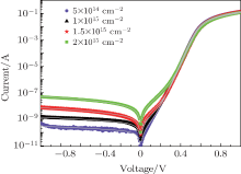
The dark current-voltage curves of boron implanted cells are shown in Fig. 5 together with the fitted lines. At each dose, the curve consists of two basic exponential components. One is an ideal (n= 1) exponential component at current densities corresponding to the solar operation, while a nonideal (2< n< 4) component with ideality factor in the range 2– 4 dominates the lower current levels. Extremely good fits to the experimental data can be obtained by applying the following equation:
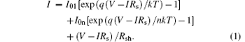
Here I01 is the saturation current density of the ideal component of current that is attributed to recombination in the cell bulk, emitter, and surfaces of the cells; I0n is the nonideal component of current related to recombination in the space charge region, where possible non-annihilated defects exist as effective recombinative centers for carriers in forward bias; Rs and Rsh are the series and the shunt resistances of the device; kT/q is the thermal voltage; and n is the ideality factor of the nonideal current component.
From the diode parameters summarized in Table 1, we notice that all the three parameters, I01, I0n, and n, are an increasing function of the implantation dose. This indicates that more recombination occurs inside the device, especially in the space charge region, as evidenced by the parameter I0n that sharply increases by two orders of magnitude. Taking into consideration the measured J0e data and the minority carrier diffusion lengths in the base to be discussed below, the increase of I01 with increasing dose can be easily understood. The bigger the parameter n is, the lower the quality of the junction exhibits, and further, the lower Voc the future solar cell will show. The large sensitivity of the nonideal component of current I0n and the ideality factor n to the implantation dose is most likely due to, according to the previous defects evolution analysis, more remnant damages present in the space charge region under higher implantation doses. These defects play key roles in degrading the junction quality of the diode in dark measurement.
 | Fig. 5. Measured dark I– V characteristics of the fabricated cells with different doses (symbols) and their corresponding fitted curves by applying the double-diode model (lines). |
| Table 1. Diode parameters obtained by fitting the dark I – V curves to Eq. (1). |
The performance parameters of the solar cells reveal pronounced distinctions between different implantation doses (Table 2). It is worth noting that these tested performance parameters are mean values of seven identically implanted cells fabricated on the same wafer and in the same batch, so that the reliability of the experimental results is greatly enhanced and uncertainty from process obviations is minimized.
It can be found from Table 2 that Voc and Jsc exhibit an obvious drop as the implantation dose increases from 5× 1014 cm− 2 to 2× 1015 cm− 2, indicating increased recombination at the device level. This trend can be preliminarily accounted for by the measured J0e results and fitted I0n parameters in the previous sections. To be specific, the degradation of the cell performance incurred by the heavier dose is largely attributed to more remnant defects inside the devices, which are not completely removed by the currently adopted isothermal annealing. Therefore, the higher thermal budget is indispensable for higher dose implantation. Also shown in the last column is implied Voc obtained by the QSSPC measurement. They follow a similar trend with the implantation dose, providing additional confirmation of the dose dependence of practical Voc. In contrast, FF is an obvious increasing function of implantation doses. This is because FF is closely related to the series resistance, which mainly includes the emitter sheet resistance and the metal– semiconductor contact resistance. On one hand, the decrease of the emitter doping concentration will directly result in an increase of the emitter sheet resistance, just as the Rsheet in the first column reveals. On the other hand, the contact resistance is also prone to increase with a decrease of surface doping concentration of the semiconductor.[23] This negative relationship is especially noticeable for the fine-line metallization scheme without locally heavy doping beneath the contact, just as in the blanket emitter investigated in this study. As a result of the more prominent reduction of Voc and Jsc, the cell efficiency shows reduction by about 0.5% absolute for every dose increase of 5× 1014 cm− 2. A maximum efficiency of 19.59% is obtained at the optimum boron ion implantation dose of 5× 1014 cm− 2 using the present annealing process. Further decrease of implantation dose below 5× 1014 cm− 2 will inevitably incur emitter sheet resistance far more than 200 Ω /⧉ , leading to a rather poor filling factor and disappointing cell performance.
| Table 2. One-sun parameters of the ion implanted solar cells with different doses. The performance parameters were tested by a solar simulator under standard terrestrial test conditions (AM1.5G, 100 mW/cm2, 25 ° C, aperture area measurement). |
The internal quantum efficiencies (IQE) of the fabricated solar cells are compared in Fig. 6. All the cells demonstrate overall high response yet apparent individual difference over a wide range of wavelength (from 360 nm to 1050 nm). The lowly doped emitter (5× 1014 cm− 2) yields a high blue response (> 80%) and near unity visible wavelength response, providing an additional evidence for the high Jsc value (39.2 mA/cm2). We can see an obviously decreased response for cells with higher implantation doses at the wavelength range shorter than 500 nm. This uncovers the cause of Jsc reduction in Table 2. It is worthwhile relating this trend to the measured J0e data in Fig. 3. From the striking consistency between the two measurements, we conclude that the passivating quality of stacking layers must have been hampered under high surface boron concentration and that some factors significantly degrading the quality of bulk emitter have taken on the effect as the implantation dose increases to higher levels. According to the mechanism analyzed in Fig. 4, there is a strong possibility that the defects limiting the shortwave response are clusters and dislocation loops located in the near surface region and the depletion region of the emitter. They act as localized states to have the photogenerated carriers annihilated, thus leading to poor internal quantum efficiency.
 | Fig. 6. Internal quantum efficiency versus wavelength for the boron implanted solar cells. The inset shows the response at wavelength between 800 nm and 1000 nm. |
According to the linear fitting method described by Green, [24] the intercept of the linear fitting equation in the lower right corner of Fig. 7 displays the minority carrier diffusion length of silicon at different doses. We can see that the hole diffusion length drops from 721.9 μ m for a 5× 1014 cm− 2 dose to 668.9 μ m for 2× 1015 cm− 2. It is therefore concluded that the bulk minority carrier lifetime has been whittled down by the implantation process or the combined process of implantation and annealing. This observed ion implantation induced lifetime degradation is supported by Macdonald's investigation on the carrier lifetime of ion-implanted silicon.[25] According to his explanation, in addition to recombination by bulk vacancy and trapping by native defects, there are other fates in terms of excess interstitials: some small fraction of interstitials avoid being bound in EOR loops or recombining at surfaces and are consequently injected into the wafer bulk. They migrate quickly to the deeper region, forming a spatially uniform distribution up to a depth of 100 μ m in the bulk silicon and acting as effective recombination centers to reduce the minority carrier lifetime. A higher dose results in a greater initial concentration of interstitials, and so a higher concentration is likely to escape into the bulk during annealing, consistent with the calculated minority carrier diffusion length results here. It is these deep penetrating defects that are extremely detrimental to the performance of devices that rely on the properties of the wafer bulk.
 | Fig. 7. Plots of 1/α versus F/η Q to determine the minority carrier diffusion length L for solar cells implanted with different doses. |
We conducted an investigation of boron implanted emitters and their applications to n-type solar cells. Some routine characterization of the boron implanted region was performed and analyzed. We firstly resorted to TCAD simulation tools to obtain the diffusion parameters of dopants and damage evolution by accurate matching of boron doping profiles between simulation and SIMS measurement. Emitter saturation current density (J0e) measurement based on the QSSPC technique presented us with some information that an increase of the implantation dose can incur significantly higher J0e than theoretically expected results. X-ray diffraction measurement of the crystallographic quality of the implanted region shows that a higher implantation dose would result in a degradation of crystallographic quality after annealing, indicating a great deal of residual damage stemming from insufficient annihilation of defects created during the high dose implantation process.
Most important to note is our reliable results of fabricated solar cells to check the emitter quality at the device level. The efficiency, in general, is a decreasing function for dose increase. The Voc and Jsc show decreasing trends with increase of the implantation dose, however, FF increases steadily with increasing dose. Dark I– V characteristics were analyzed by the double-diode fitting technique. From the obtained fitting parameters, it is known that a large non-ideal component of saturation current degraded the junction quality. Internal quantum efficiency diagnosis of the devices showed that both blue and infrared responses were greatly affected by the dose increase. Secondary extended defects like clusters and dislocation loops that appear at high implantation doses are the possible performance limiting factors because they greatly increase the overall recombination rate in the internal device.
| 1 |
|
| 2 |
|
| 3 |
|
| 4 |
|
| 5 |
|
| 6 |
|
| 7 |
|
| 8 |
|
| 9 |
|
| 10 |
|
| 11 |
|
| 12 |
|
| 13 |
|
| 14 |
|
| 15 |
|
| 16 |
|
| 17 |
|
| 18 |
|
| 19 |
|
| 20 |
|
| 21 |
|
| 22 |
|
| 23 |
|
| 24 |
|
| 25 |
|