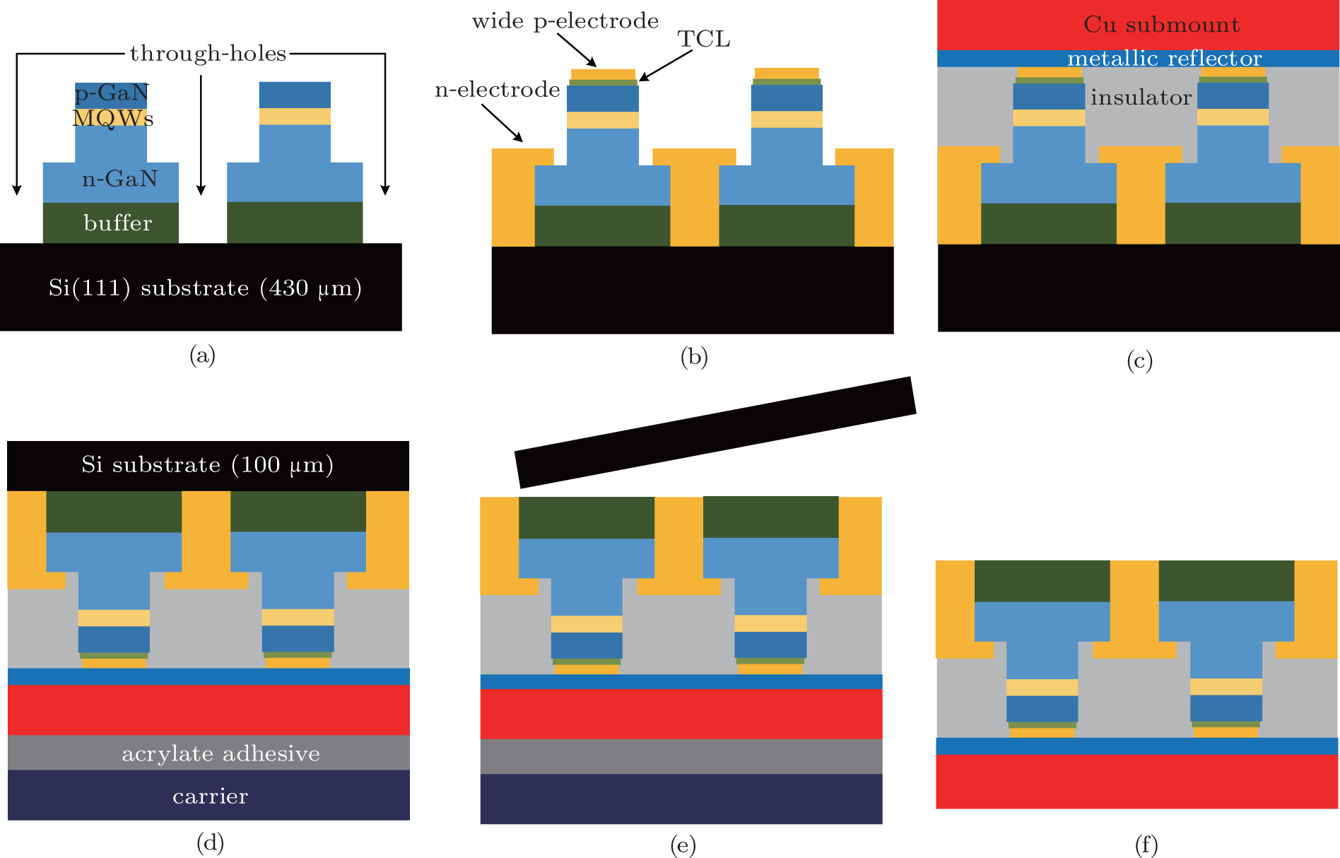
Performance improvement of GaN-based light-emitting diodes transferred from Si (111) substrate onto electroplating Cu submount with embedded wide p-electrodes*
Liu Ming-Gang†, Wang Yun-Qian†, Yang Yi-Bin†, Lin Xiu-Qi, Xiang Peng, Chen Wei-Jie, Han Xiao-Biao, Zang Wen-Jie, Liao Qiang, Lin Jia-Li, Luo Hui, Wu Zhi-Sheng, Liu Yang, Zhang Bai-Jun‡
       
Device fabrication processes of the embedded wide p-electrode LED on Cu submount: (a) etch to form the LED mesas and through-holes by ICP-RIE, (b) deposit TCL, wide p-electrode and metals filled into through-holes forming n-electrode, (c) isolate n- and p-electrodes by the insulator, deposit Cr/Al/Pd/Au metals as a metallic reflector onto the wide p-electrode surface, and electroplate a 100-μm-thick Cu layer, (d) bond the wafer to a temporary substrate using the acrylate adhesive and thin the Si substrate, (e) remove Si substrate by wet-chemical etching, (f) separate the devices from the temporary substrate and form embedded wide p-electrode LEDs on Cu.