


A novel integrated ultraviolet photodetector based on standard CMOS process*
[Wang Hana), b) , Jin Xiang-Lianga), b)†  , Chen Chang-Ping
a), b) , Tian Man-Fanga), b) , Zhu Ke-Hanc) ]
, Chen Chang-Ping|
|


†Corresponding author. E-mail: jinxl@xtu.edu.cn
*Project supported by the National Natural Science Foundation of China (Grant No. 61274043), the Key Project of the Ministry of Education of China (Grant No. 212125), and the State Key Program of the National Natural Science Foundation of China (Grant No. 61233010).
A novel integrated ultraviolet (UV) photodetector has been proposed, which realizes a high UV selectivity by combining a conventional UV-selective photodiode with an extra infrared (IR) photodiode. The IR photodiode is designed for compensating the photocurrent response of the UV photodiode in the infrared band and is 15 times smaller than the UV one. The integrated photodetector has been fabricated in a 0.35 μm standard CMOS technology. Some critical performance indices of this new structure photodetector, such as spectral responsivity, breakdown voltage, quenching waveform, and transient response, are measured and analyzed. Test results show that the complementary UV–IR photodetector has a maximum spectral responsivity of 0.27 A·W−1 at the wavelength of 400 nm. The device has a high UV selectivity of 3000, which is much higher than that of the single UV photodiode.
The ultraviolet (UV) detector is an emerging research topic. It is widely used in biology, medicine, flame detection, space-to-space communications, and environmental monitoring.[1– 5] The operation principle behind these applications is that a detector transforms the response produced by the weak light signal in a narrow wavelength range into an electrical signal to realize the acquisition of the signal. Therefore, the device should at least have high sensitivity and high wavelength selectivity for achieving a better performance. The photodetector made of wide-bandgap materials, such as SiC and GaN, has higher responsivity and better wavelength selectivity.[6– 10] Nevertheless, they are endowed with poor stability and are not compatible to the microelectronic process, which result in the limited practical applications.
Silicon-based photodetectors can not only overcome the above disadvantages, but also have the advantages of low cost and low power consumption. Hence, they attract a great deal of attention in academia and industry. However, the cutoff wavelength of silicon is 1100 nm and each band implants a different depth in silicon, which lead to poor wavelength selectivity and poor sensitivity for ordinary photodiodes. To overcome the disadvantages of the conventional photodiodes, better structures of the device should be designed. Different structures have been presented to enhance the responsivity and improve the selectivity of the silicon photodiode. A silicon stripe-shaped photodiode[11] achieves better selectivity by using a shallow active region, the stripe-shaped structure is used to make the area of the dead layer as small as possible and thus improves the sensitivity of the UV photodiode. A P+ – I– N+ junction-surface depletion-layer photodiode[12] shows good responsivity, with a quantum efficiency of nearly 56% at λ = 400 nm, however the maximum is located at the wavelength of 920 nm, which means that there is no selectivity for this photodiode. A UV-enhanced photodiode[13] has a responsivity of 0.23 A· W− 1 at λ = 400 nm with nine-fingers. An ultra-shallow-junction silicon photodiode achieves excellent UV selectivity in the UV spectral range, [14] however a high supply voltage is needed. A novel monolithic ultraviolet image sensor based on a standard CMOS process[15] is designed with a floating gate, and this image sensor can only absorb strong ultraviolet radiation. In this paper, a new integrated photodetector for UV radiation detection is presented. It consists of a conventional UV-selective photodiode and an extra infrared (IR) photodiode. The IR photodiode is 15 times smaller than the UV one and is used to decrease the photocurrent response of the photodetector when illuminated in the IR range.[4] A smart combination of UV and IR photodiodes makes the proposed photodetector not only sensitive to the UV radiation, but also have a higher UV-selectivity than the traditional silicon-based single UV photodiode.
In this paper, we present a new complementary UV photodetector, which can enhance the UV selectivity. The photodetector structure and its operation principle are presented in the next section. The measurement circuit and system are described in Section 3. The results are presented in Section 4. Section 5 concludes this study.
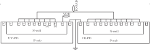
In this study, we aim at enhancing the UV selectivity of the silicon-based UV photodiode. It could be enhanced by using optical filters, but a low-cost alternative is preferred. We propose a compensation method. A small IR photodiode, as shown in Figs. 1 and 2, is added to the UV photodetector. As the UV photodiode has smaller responsivity in the IR range, the area of the IR photodiode should be 15 times smaller than that of the UV one. An appropriate ratio of the photodiode areas is kept in order to match the optical responses of the two photodiodes as close as possible in the IR range. Meanwhile the UV and the IR photodetectors possess similar cross sections, as illustrated in Fig. 1. It is actually a conventional P+ – Nwell– Psub structure, while the body (substrate) is a P+ guard ring; it consists of several P+ type anodes, which are implemented by boron implantation in Nwell, all P+ stripes of both the UV and IR photodiodes are connected together through metal.
 | Fig. 1. Cross section of the UV photodetector. |
The difference between the UV photodiode and the IR photodiode (PD) lies in the connection, as shown in Fig. 1. For IR-PD, the upper P+ – Nwell junction is short-circuited to make the photodiode have no response for the UV radiation and collect only the photocurrent produced by the Nwell– Psub junction. While for UV-PD, the upper P+ – Nwell junction is valid; it is also the focus of this study. The high UV selectivity of the photodiode results from the combined effect of the wavelength-dependent light absorption coefficient. Electron– hole pairs are created within the P+ anode because UV photons have a penetration depth of smaller than 100 nm. Electrons, which are driven by a built-in electric field due to the nonuniform doping profile, enter the high-field region of the p+ – n junction at a depth of 140 nm and form the electronic diffusion current.[16] To gather most UV information assimilated by the upper P+ – Nwell junction, which is due to the complete overlap of the lateral space depletion region between two P+ anodes. Parameters d and w are chosen to be 3.0 μ m and 3.86 μ m, respectively.
The equivalent circuit of our UV photodetector is displayed in Fig. 2. When the photodetector is exposed to light, the photocurrent IUV of the UV photodiode includes the information from the ultraviolet signal and a small amount of infrared and visible information. The visible information produced by the Nwell– Psub junction directly flows to GND. Similarly, the infrared and visible information produced by the IR diode directly flows to GND. When the photodetector is exposed to IR radiation, the photocurrent IIR of the IR photodiode is from the parasitic photocurrent IUV produced by the UV photodiode.[4] Thus the photocurrent response of this photodetector decreases in the IR range, and a clean photocurrent Iph = IUV − IIR is achieved.
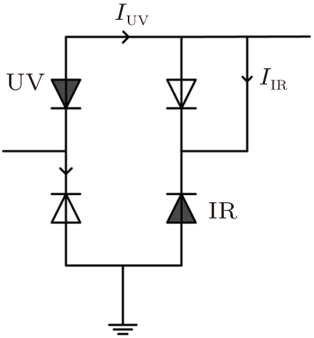 | Fig. 2. Equivalent circuit of the UV photodetector. |
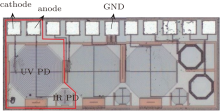
The whole chip, as shown in Fig. 3, was fabricated with a standard 0.35 μ m technology. The UV photodetector presented in this study lies in the left region of the red line. It consists of a 0.6 mm2 UV PD and an IR PD which is 15 times smaller to achieve a high UV selectivity. It includes three electrodes, cathode, anode, and GND. Obviously, all devices of this chip share the same GND. For both UV PD and IR PD, the Psubstrate is connected directly with GND. All N+ cathodes of the UV PD are connected through metal to form a cathode electrode. The anode electrode is connected with the P+ anodes of the UV PD, the P+ anodes of the IR PD, and the N+ cathodes of the IR PD. For the IR PD, all P+ anodes and N+ cathodes are connected together, so the P+ – Nwell junction is short-circuited, and the photodiode has no response in the UV range, which could help to have a better compensating photocurrent response in the infrared band.
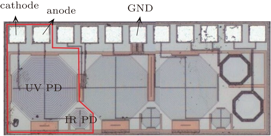 | Fig. 3. Photograph of the UV photodetector. |
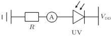
APD photodiode tester (GCAPD-B), oscilloscope (Tektronik MSO-2024), and a high precision amperemeter were used to test the proposed photodiode. Detailed measurements and comparisons will be analyzed and discussed below. The spectral responsivity and electrical property of both a single UV photodiode and a complementary UV photodetector were measured using the test circuits in Figs. 4 and 5, respectively. As shown in Fig. 4, the cathode and the anode of the single UV photodiode are connected to VDD and the high precision amperemeter (with a precision of fA), respectively. The high precision amperemeter is connected to the ground through a resistor R and it will give the photocurrent of the single UV PD. In Fig. 5, the UV photodiode, the IR photodiode, and a resistor R1 are connected in series. The high precision amperemeter series connected with a resistor R2 is connected in parallel with the IR photodiode. The signal acquired by the high precision amperemeter in Fig. 5 is the effective photocurrent Iph = IUV − IIR and it is equivalent to the photocurrent of the UV photodetector.
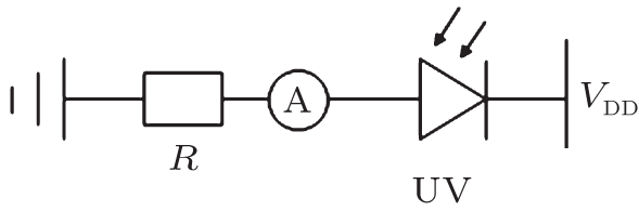 | Fig. 4. Test circuit for the single UV PD. |
 | Fig. 5. Test circuit for the proposed UV photodetector. |
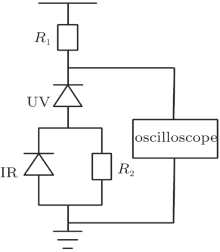
The transient response of the UV photodetector was measured with the circuit shown in Fig. 6. The bandwidth and the sampling rate of the mixed signal oscilloscope are 200 MHz and 1 Gs− 1, respectively. The R1 is 1 MΩ and R2 is 20 MΩ . The wavelength range of the light source used in the measurement is from 300 nm to 1000 nm. For convenience, just some special wavelengths were chosen for testing, such as 350 nm, 420 nm, 500 nm, 650 nm, 750 nm, 800 nm, 900 nm, 1000 nm, and so on.
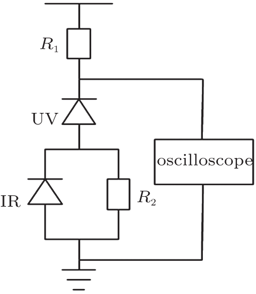 | Fig. 6. Test circuit for transient response. |
Figure 7 shows the product of the responsivity and the photodiode area for both the single UV photodiode and the UV photodetector. In the blue/UV range, the responsivity– area product of the UV photodiode achieves its maximum, whereas that of the IR photodiode is negligible. On the contrary, for λ > 850 nm, thanks to the appropriate ratio of the photodiode areas, the product of the IR photodiode is almost equal to that of the UV photodiode.
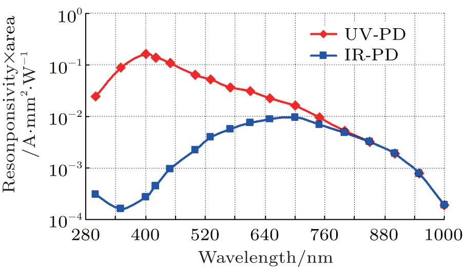 | Fig. 7. Product of the measured responsivity and the active area versus the wavelength for the UV PD and the IR PD. |
To achieve a high UV selectivity with this method, it is essential that the photocurrents produced by the two photodiodes are equal in the NIR range. A too large IR photodiode area would result in an overcompensation of the parasitic UV photodiode photocurrent and lead to a detrimental negative system response in the NIR range.
Figure 8 compares the spectral responsivity of the single UV PD with that of the complementary UV photodetector, where the optical power is 1.34 μ W. The UV photodetector obtains a maximal responsivity of 0.27 A· W− 1 when the radiation wavelength is 400 nm. In the UV region, its spectral responsivity is equal to that of the single one. While in the VIS and NIR ranges, its spectral responsivity drops rapidly. In this paper, we define the UV selectivity as the ratio between the responsivity at the wavelength of maximal response and that at λ = 1 μ m. Figure 8 shows clearly that the UV photodetector obtains a UV selectivity of 3000 while the single UV PD only has a selectivity of 860. The extra infrared photodiode is proved to be the right move for improving the performance of the device. In a word, both the intrinsic selectivity of the UV photodiode and the addition of the IR photodiode help to obtain a higher UV selectivity.
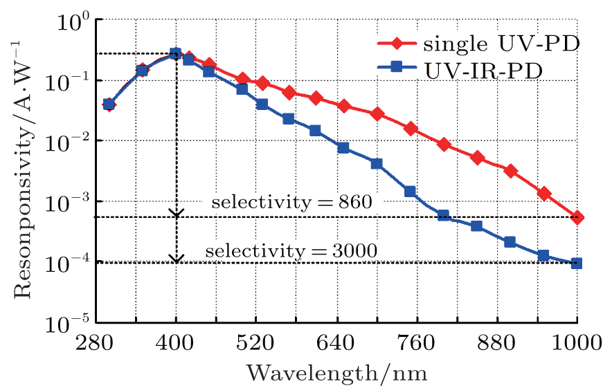 | Fig. 8. The spectral response curves of the single UV PD and the UV photodetector at an optical power of 1.34 μ W. |
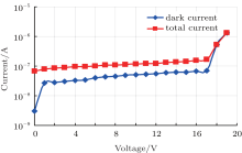
Both the dark current and the total current were measured. Figure 9 shows the results. A dark current of 3 × 10− 9 A at a voltage of 0 V and a photocurrent of 8.5 × 10− 8 A at a voltage of 1 V have been measured at the wavelength of 700 nm (white light, 800 lx). The results indicate a low enough dark current for the device, which is important for proving the performance. The breakdown voltage is 16.8 V for the UV photodetector.
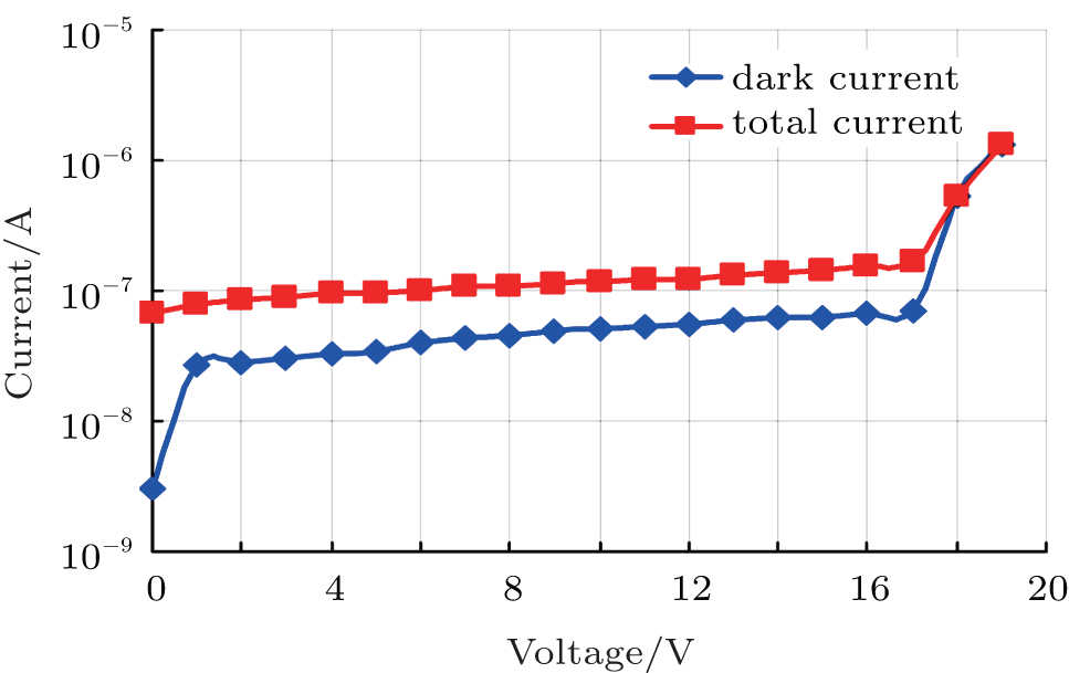 | Fig. 9. Measured I– V characteristics under dark and illumination conditions. |
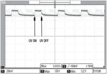
The same test circuit shown in Fig. 6 was used for obtaining the quenching waveform and the response waveform. The quenching waveform describes the change of voltage across the resistor R1, while the response waveform represents the change of voltage across the UV-IR photodetector. The results obtained by the oscilloscope are displayed in Figs. 10 and 11.
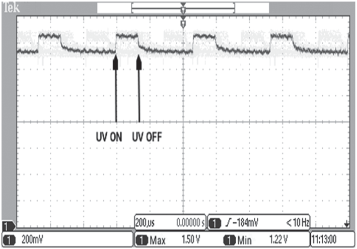 | Fig. 10. Quenching waveform of the UV photodetector. |
 | Fig. 11. Transient response of the UV photodetector. |
The voltage drop on resistor R1 is V1 = Idark × R1 when there is no light pulse. Once a light pulse comes, the voltage drop on R1 becomes V2 = Itotal × R1, which is larger than V1. When the light pulse vanishes, the photocurrent gradually decreases, and a quenching process appears. The output swing is about 280 mV, and a rise time of 10 μ s and a fall time of 12 μ s are obtained.
The response time represents the speed of the ultraviolet photodiode under a bias voltage and favorable light conditions. The output swing is about 340 mV, while the rise time and the fall time are both 12 μ s.
A novel integrated UV photodetector for ultraviolet radiation detection has been presented, which is fabricated in a standard 0.35 μ m CMOS technology. The photosensitive part of this photodetector consists of an IR photodiode and a 15 times larger UV-selective photodiode, the IR photodiode is designed for compensating the photocurrent response of the UV photodiode in the infrared band. The complementary UV photodetector has a low breakdown voltage of 16.8 V and a high transient response. It achieves a maximum spectral responsivity of 0.27 A· W− 1 at λ = 400 nm. The proposed complementary UV photodetector shows a higher UV selectivity of 3000. The result shows that the addition of an infrared photodiode improves the UV selectivity by nearly 2.5 times.
| 1 |
|
| 2 |
|
| 3 |
|
| 4 |
|
| 5 |
|
| 6 |
|
| 7 |
|
| 8 |
|
| 9 |
|
| 10 |
|
| 11 |
|
| 12 |
|
| 13 |
|
| 14 |
|
| 15 |
|
| 16 |
|