


Effect of helium implantation on SiC and graphite*
[Guo Hong-Yana), b)† , Ge Chang-Chuna), b)‡  , Xia Min
b)†§ , Guo Li-Pingc) , Chen Ji-Hongc) , Yan Qing-Zhib) ]
, Xia Min, Guo Li-Ping|
|


†These authors contributed equally to this work.
‡Corresponding author. E-mail: ccge@mater.ustb.edu.cn
§Corresponding author. E-mail: xmdsg@126.com
*Project supported by the ITER-National Magnetic Confinement Fusion Program, China (Grant Nos. 2010GB109000, 2011GB108009, and 2014GB123000) and the National Natural Science Foundation of China (Grant No. 11075119).
Effects of helium implantation on silicon carbide (SiC) and graphite were studied to reveal the possibility of SiC replacing graphite as plasma facing materials. Pressureless sintered SiC and graphite SMF-800 were implanted with He+ ions of 20 keV and 100 keV at different temperatures and different fluences. The He+ irradiation induced microstructure changes were studied by field-emission scanning electron microscopy (FESEM), atomic force microscopy (AFM), and transmission electron microscopy (TEM).
Plasma facing materials and components (PFM/PFC) not only play a key role but also are the greatest technically difficult parts in magnetic constraint fusion devices.[1] PFM/PFC should withstand 14 MeV neutrons, high-intensity plasma flow, high-intensity heat flux, and helium, deuterium, tritium and other particles erosion. At present, graphite is widely used in fusion plasma devices. However, carbon possesses high chemical reactivity with hydrogen and oxygen, which is considered to be a fatal drawback.[2– 4] Thus, attempts are being made to explore new PFM/PFC. As one of the most perspective candidate materials, W-based PFM/PFC is now widely studied and suggested for future fusion reactors. However, its shortcomings, such as high ductile-to-brittle transition temperature (DBTT), low recrystallization temperature, and neutron irradiation brittleness, may depress its availability as plasma facing components.[5] Thus we should not neglect other strategies. As a low atomic number (Z) compound, silicon carbide (SiC) has a series of advantages in fusion reactors, such as low contamination to plasma, good high-temperature properties, high corrosion resistance, low density, and especially the environmentally benign property of low-induced radioactivity after neutron irradiation.[6– 10] We have revealed that the SiC surface presents slight damage after Tokomak in situ plasma irradiation (66 times discharges), the chemical sputtering of SiC is one order lower than that of nuclear graphite SMF-800, and the thermal desorption ratio is about 10% of graphite.[11– 13]
As an extension of the previous work in our group, SiC and bulk graphite materials with sizes about 10 mm× 10 mm× 0.5 mm, 10 mm× 20 mm× 0.5 mm and transmission electron microscopy (TEM) lamellas were implanted by He+ ions in the present study. Microstructures such as helium bubbles and micro-voids, and the relationship between the microstructure changes and the irradiation temperatures and doses were studied. Based on our previous work and the new results shown in this work, the possibility of SiC replacing graphite as future first wall materials and PFC is further verified.
Pressureless sintered SiC and graphite SMF-800 were used in this study. Mechanical polished and ultrasonic cleaned bulk samples with sizes about 10 mm× 10 mm× 0.5 mm and 10 mm× 20 mm× 0.5 mm were prepared before implantation. TEM lamellas with diameter about 3 mm were prepared using the ion milling technique.
Helium micro-bubbles or micro-voids on SiC surfaces induced by He+ ion irradiation were studied using the heavy ion research facility in Lanzhou (HIRFL) and the accelerator in the School of Physics and Technology of Wuhan University. Incident energies of 20 keV and 100 keV, as well as room temperature (RT) and 600° C were selected to study the energy and temperature effects. Details of the irradiation experiments are shown in Table 1. Scanning electron microscopy (SEM) was employed to characterize the microstructure change. The surface roughness was determined by atomic force microscopy (AFM), and the helium bubble feature was studied using TEM.
| Table 1. He+ ion implantation fluencies and incident energies in the experiments. |
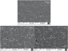
To study the microstructure change on the surface, bulk graphite and SiC were irradiated by 100 keV He+ ions with a fluence of about 1017 cm− 2 (Lanzhou, HIRFL) at RT and 600° C. Figure 1 gives the surface morphology of bulk graphite before and after the He+ implantation. Figure 1(a) is the surface image of graphite SMF-800; as can be seen, many shallow holes and micro-holes are detected on the surface, which are typical features of graphite. Figures 1(b) and 1(c) are the surface images of the graphite irradiated at 600° C and RT; both images show that the holes on the surface are deepened and enlarged, and the density of holes is increased obviously. Besides, many small cracks and fragments caused by collapse are detected on the surface of the graphite after the He+ implantation at RT.
 | Fig. 1. Morphology of the graphite before and after He+ implantation: (a) before He+ implantation, (b) He+ implantation at 100 keV, 1017 cm− 2, 600° C, and (c) He+ implantation at 100 keV, 1017 cm− 2, RT. |
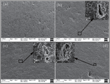
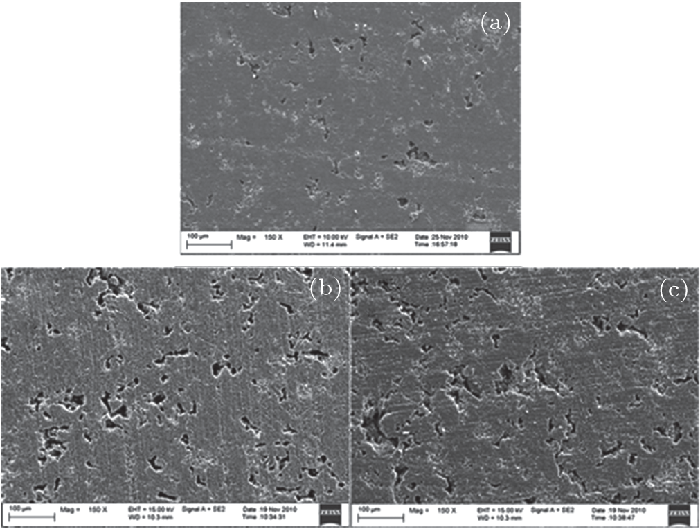
In the case of SiC, the surface of SiC shows less changes after the He+ implantation under the same implantation conditions, as shown in Fig. 2. Figure 2(a) is the surface image of the un-implanted SiC. It is found that some small defects on the surface of the specimen are enlarged into elliptical micro-voids with size about 2 μ m× 5 μ m, while individual original voids of 1– 2 μ m develop into large voids of ø 2– 5 μ m× 10– 15 μ m (Fig. 2(b)-2(d) inset), which is significantly different from that of graphite under the same condition of He+ implantation. The results indicate the excellent sputtering resistance of SiC compared with graphite SMF7-800.
 | Fig. 2. Morphology of SiC before and after He+ implantation: (a) before He+ implantation, (b) He+ implantation at 100 keV, 1017 cm− 2, 600° C, (c) (d) He+ implantation at 100 keV, 1017 cm− 2, RT. |
To study the density and diameters of helium bubbles after He+ implantation, graphite SMF-800 and SiC TEM lamellas were directly implanted with the fluence and energy of He+ ions of 3× 1016 cm-2 and 100 keV at 600° C (with the accelerator in Wuhan University). Figures 3(a) and 3(b) are the TEM morphologies of He+ implanted graphite SMF-800, high-density of helium bubbles with diameters about 10– 20 nm are observed. Figures 3(c) and 3(d) are the typical images of He+ implanted SiC, the density of helium bubbles (white arrows indicated in Fig. 3(d)) in SiC is lower than that in graphite, and the diameters detected are about 2– 8 nm. The dark spots in Figs. 3(c) and 3(d) are surface artifacts induced by specimen preparation. The results of TEM observations indicate the excellent and better He+ radiation resistance of SiC than that of graphite SMF-800.
 | Fig. 3. TEM images of He+ implanted TEM lamella at 600° C: (a), (b) Graphite SMF-800; (c), (d) SiC. |
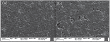
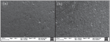
Figures 4 and 5 show the morphology of graphite before and after 20 keV He+ implantation at RT and 600° C with the fluence of 2× 1017 cm− 2. Figures 4(a) and 5(a) are the images of un-irradiated graphite; many shallow holes and micro-holes are detected on the surface, which is consistent with the surface morphology described in Fig. 1(a). The typical surface changes of graphite after helium implantation are recorded in Figs. 4(b) and 5(b). As can be seen, the graphite surface shows no obvious change before and after the He+ implantation at RT in Fig. 4(b). However, when the temperature rises up to 600° C (Fig. 5(b)), many small cracks and fragments caused by collapse are observed on the surface of the graphite, and the diameters and density of the holes are enlarged.
 | Fig. 4. Morphology of graphite (a) before and (b) after 20 keV He+ implantation with the fluence of 2× 1017 cm− 2 at RT. |
 | Fig. 5. Morphology of graphite (a) before and (b) after 20 keV He+ implantation with the fluence of 2× 1017 cm− 2 at 600° C. |
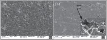
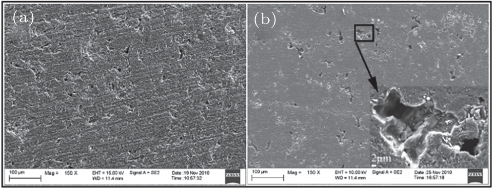
Figures 6 and 7 are the typical surface profiles of SiC with and without 20 keV He+ implantation with the fluence of 2× 1017 cm− 2 at RT and 600° C. Figures 6(a) and 6(b) are pressureless sintered SiC without He+ implantation at RT and 600° C, It can be seen that there are no obvious surface changes under low energy implantation in SiC at different temperatures.
 | Fig. 6. Morphology of SiC (a) before and (b) after 20 keV He+ implantation with the fluence of 2× 1017 cm− 2 at RT. |
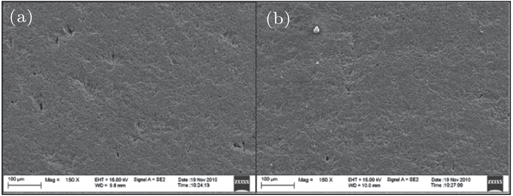 | Fig. 7. Morphology of SiC (a) before and (b) after 20 keV He+ implantation with the fluence of 2× 1017 cm− 2 at 600° C. |
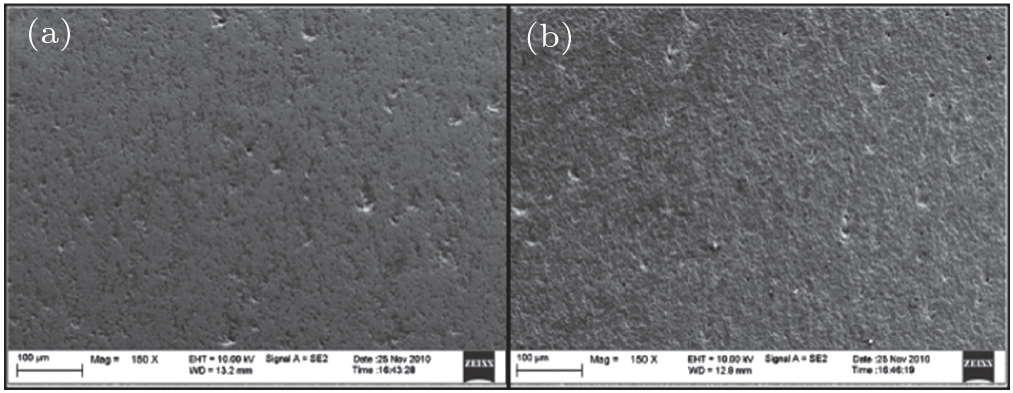
Since no obvious surface changes of SiC (at RT and 600° C) were observed under the energy of 20 keV, AFM process was applied to further study the surface roughness changes of SiC after the He+ implantation. Figure 8(a) gives the original AFM images of SiC before the He+ implantation. Figures 8(b) and 8(c) are the morphologies of SiC after 20 keV He+ implantation with the fluence of 2× 1017 cm− 2 at RT and 600° C. The results reveal that the arithmetic mean roughness (Ra) rises from 42.3 nm (Fig. 8(a)) to 46.6 nm (Fig. 8(b)) at RT and to 54.2 nm (Fig. 8(c)) at 600° C after the He+ implantation. AFM data of SiC further demonstrate the slight surface profile changes.
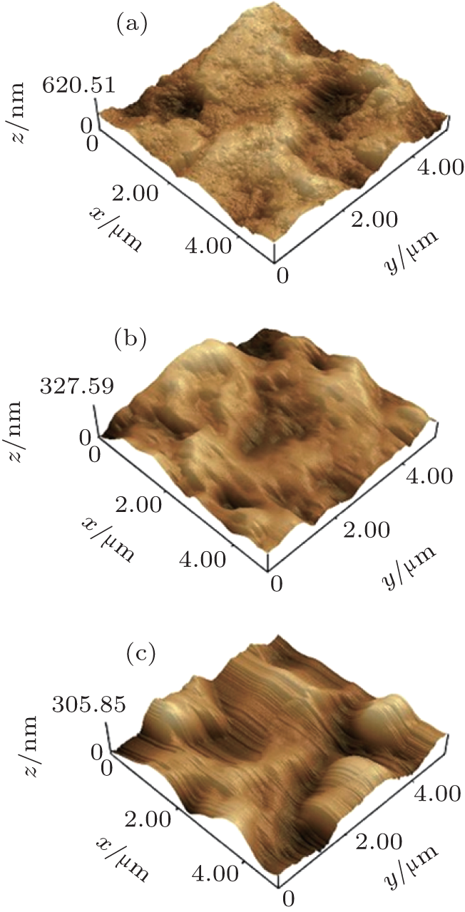 | Fig. 8. AFM images of bulk SiC before and after He+ implantation: (a) before He+ implantation, (b) He+ implantation at RT, (c) He+ implantation at 600° C. |
The results show that the microstructure changes on SiC are much less than those of He+ implantation on graphite SMF-800 even at different temperatures and doses. About 10∼ 20 μ m voids, 5– 10 nm helium bubbles, clusters of small cracks, and many fragments caused by collapse are detected on the surface of SMF-800 after He+ implantation. However, no obvious surface change is observed in SiC, except for the slight surface roughness change. Combined with our previous results, less obvious plasma irradiation damage, excellent erosion resistance, high hot shock resistance, and high heat conductivity of SiC indicate that it is much more perspective to be the first wall materials and plasma facing components for the future fusion facilities and reactors.
| 1 |
|
| 2 |
|
| 3 |
|
| 4 |
|
| 5 |
|
| 6 |
|
| 7 |
|
| 8 |
|
| 9 |
|
| 10 |
|
| 11 |
|
| 12 |
|
| 13 |
|