Du Yan-Ling, Wang Chun-Lei, Li Ji-Chao, Zhang Xin-Hua, Wang Fu-Ning, Liu Jian, Zhu Yuan-Hu, Yin Na, Mei Liang-Mo. Two-dimensional metallic behavior at polar MgO/BaTiO3 (110) interfaces* . Chinese Physics B, 2015, 24(3): 037301
Permissions
Two-dimensional metallic behavior at polar MgO/BaTiO3 (110) interfaces*
Du Yan-Linga),b), Wang Chun-Leia), Li Ji-Chaoa)†, Zhang Xin-Huaa), Wang Fu-Ninga), Liu Jiana), Zhu Yuan-Hua), Yin Naa), Mei Liang-Moa)
School of Physics, Shandong University, Jinan 250100, China
College of Science and Technology, Shandong University of Traditional Chinese Medicine, Jinan 250355, China
Project supported by the National Basic Research Program of China (Grant No. 2013CB632506), the National Natural Science Foundation of China (Grant Nos. 11374186, 51231007, 51202132, and 51102153), and the Independent Innovation Foundation of Shandong University, China (Grant No. 2012TS027).
Abstract
The first-principles calculations are employed to investigate the electrical properties of polar MgO/BaTiO3 (110) interfaces. Both n-type and p-type polar interfaces show a two-dimensional metallic behavior. For the n-type polar interface, the interface Ti 3d electrons are the origin of the metallic and magnetic properties. Varying the thickness of BaTiO3 may induce an insulator–metal transition, and the critical thickness is 4 unit cells. For the p-type polar interface, holes preferentially occupy the interface O 2p y state, resulting in a conducting interface. The unbalance of the spin splitting of the O 2p states in the interface MgO layer leads to a magnetic moment of about 0.25 μB per O atom at the interface. These results further demonstrate that other polar interfaces, besides LaAlO3/SrTiO3, can show a two-dimensional metallic behavior. It is helpful to fully understand the role of polar discontinuity on the properties of the interface, which widens the field of polar-nonpolar interfaces.
Keyword:
73.20.At; 75.70.Cn; 73.20.–r; 75.70.–i; electronic structures; MgO/BaTiO3 (110) polar interfaces; two-dimensional electron gas (2DEG); magnetism
Since a high-mobility electron gas was discovered at the LaAlO3/SrTiO3 interface, [1] much effort has been devoted to reveal its origin. Many researchers have investigated the roles of many factors, including oxygen vacancies, [2, 3] chemical intermixing, [4] the thickness of the LaAlO3 sheets, [5, 6] the external electric field, [7– 9] and the epitaxial strain.[10] Besides them, the polarity discontinuity at the interface has been considered to be the dominant mechanism behind the phenomenon.[1, 11– 15] In LaAlO3/SrTiO3(001) heterostructures, the atomic layers in SrTiO3 are nominally charge neutral, whereas the atomic layers in LaAlO3 can be represented by alternating (LaO)+ and (AlO2)− layers in principle. Therefore, a polar discontinuity is expected at the interface between SrTiO3 and LaAlO3. In order to stabilize this discontinuity, it has been suggested that an extra 0.5 electron per two-dimensional unit cell is transferred from LaAlO3 (SrTiO3) to SrTiO3 (LaAlO3) in the n (p)-type interface. This model has been supported by atomic-scale electron energy-loss spectroscopy (EELS) measurements, which show that the n-type interface can be realized by the mixed valency of Ti, whereas the p-type interface can be realized by oxygen vacancies.[16]
In order to examine whether the role of the polar discontinuity at the interface is general, or unique to the LaAlO3/SrTiO3 interface, researchers have grown other superlattices with a mismatch between polar and nonpolar layers.[17– 19] Hotta and his cooperator[17] investigated the transport properties of LaVO3/SrTiO3 heterointerfaces, and found that the n-type VO2/LaO/TiO2 interface is conducting, while the p-type VO2/SrO/TiO2 interface is insulating, similar to that in LaAlO3/SrTiO3. Wang et al.[18] studied the LaAlO3/EuO(001) interface, and demonstrated that the mechanism responsible for the two-dimensional electron gas (2DEG) at the interface is similar to that for the LaAlO3/SrTiO3 interface. Perna et al.[19] investigated heterostructures based on a different overlayer. They replaced LaAlO3 with LaGaO3 and found a highly conductive interface. All the above results demonstrate that other polar interfaces, besides LaAlO3/SrTiO3, can be metallic and generate a 2DEG at the interfaces.
In this paper, we investigate the electronic structures of polar MgO/BaTiO3 (110) interfaces, in which a nonperovskite MgO (110) film is adopted as a capping layer on the BaTiO3 (110) substrate. Along the [110] direction, BaTiO3 can be represented by planar stacks of [BaTiO]4 + and [O2]4 − layers, while MgO is composed of neutral layers. Similar to the LaAlO3/SrTiO3 interface, the polar discontinuity at the MgO/BaTiO3 (110) interface needs to be compensated by electron transfer. Thus, the MgO/BaTiO3 (110) interface is expected to be conductive. As is well known, both MgO and BaTiO3 are wide band-gap insulators. The rocksalt MgO has a lattice constant of 4.21 Å , [20] while the lattice constant of BaTiO3 with the perovskite cubic structure is 4.00 Å , [21] so there is a little lattice mismatch between MgO and BaTiO3. Due to its broad applications in capacitors[22] and electro-optical devices, [23, 24]BaTiO3/MgO (001) has attracted much attention, and been fabricated using magnetron sputtering, [25– 27] chemical vapor deposition, [28] and pulsed laser deposition.[23, 29] However, there are few studies about the polar MgO/BaTiO3 (110) interfaces. Investigating the relaxation and electronic structures of the polar MgO/BaTiO3 (110) interfaces not only is helpful to fully understand the role of the polarity discontinuity on the properties of the interface but also adds to the understanding of the MgO/BaTiO3 interface.
2 Model and method
In this paper, a thin MgO film deposited on the BaTiO3 (110) substrate is modeled by (MgO)8/(BaTiO3)5 (110) heterostructures, containing 8 unit cells (four layers) of MgO and 5 unit cells of BaTiO3 within the heterostructures. Along the [110] direction, BaTiO3 can be represented by planar stacks of [BaTiO]4 + and [O2]4 − layers, resulting in two types of terminations: O2-termination and BaTiO-termination. In the case of MgO, it is composed of [MgO]0 charge-neutral stacks along the [110] direction. Thus, two polar interfaces are possible: the n-type MgO/BaTiO interface and the p-type MgO/O2 interface. As far as the thermodynamic stability is concerned, we choose the interface structure with the lowest energy. To model the MgO ultrathin film deposited on the BaTiO3 substrate, atoms in the lowest two layers of the heterostructures are fixed, and other atoms fully relax. The in-plane lattice constants of the heterostructures are fixed to those of BaTiO3. For cubic BaTiO3, we obtain a lattice constant of 3.953 Å within LDA, which is very close to the experimental value of 4.00 Å [21] and other theoretical results of 3.951 Å [30] and 3.958 Å .[31] Thus, the in-plane lattice constants a and b of the heterostructures are fixed at 3.953 Å and 5.59 Å , respectively. For cubic MgO, we obtain a lattice constant of 4.15 Å within LDA, which is very close to the experimental value of 4.21 Å .[20, 32] Thus, to modulate the thin layers of BaTiO3 grown on the top of the MgO substrate, the in-plane lattice constants a and b of the heterostructures are fixed at 4.15 Å and 5.59 Å , respectively. A vacuum spacing of 10 Å between adjacent slabs is included in each of the heterostructures to minimize the interaction between neighboring surfaces.
In this work, the first-principles density functional calculations are performed using the Vienna ab initio simulation package (VASP).[33, 34] The ion– electron interactions are described by using the projector augmented wave (PAW) method, [35] and the local density approximation (LDA) is used for the exchange– correlation energy of electrons.[36] Calculations are performed using a 5× 4× 1 Monkhorst– Pack[37]k-point mesh and a kinetic energy cutoff of 500 eV. The atoms except those in the lowest two layers are fully relaxed until the forces on the ions are less than 0.01 eV/Å .
3 Results and discussion
3.1 The n-type interface
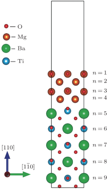
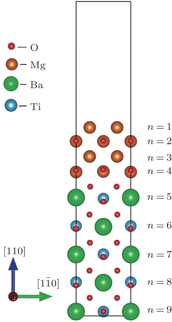
We investigate the n-type MgO/BaTiO (110) interface in the (MgO)8/(BaTiO3)5 heterostructures. Figure 1 shows the relaxed n-type MgO/BaTiO (110) interface. From the figure, we can see that the relaxation of the MgO slab is inconspicuous. Because the in-plane lattice constant of MgO is larger than that of BaTiO3, the MgO slab is under compressive strain. It is expected that the lattice constant of the relaxed MgO slab along the [110] direction would be larger than that before relaxation. However, the change is not obvious, the lattice constant of MgO along the [110] direction becomes 1.04 times of that before relaxation. In contrast to the unconspicuous relaxation in the MgO slab, the displacements of atoms in the BaTiO3 slab are significant: Ti and Ba atoms relax away from the interface, while O atoms relax close to the interface. A more thorough insight can be obtained by analyzing the relative displacements between M (M denotes Ba, Ti, or Mg) and O atoms, which are listed in Table 1. From the table, we can see that the relaxations of both Mg and O atoms in the surface MgO layer are similar, resulting in only a small buckling of 0.03 Å . The largest structural relaxation occurs in the interface BaTiO layer, and the relative displacement between O and Ba atoms results in a big buckling of 0.60 Å . The relative displacement between O and Ti (Ba) ions results in a polarization P pointed away from the interface, which can reduce the built-in potential in the BaTiO3 (110) slab[38] and the instability of the polar interface. In addition, the distortion of the Ti– O octahedrons can lead to the splitting of the Ti 3d obitals and the electronic reconstruction at the polar n-type MgO/BaTiO (110) interface.
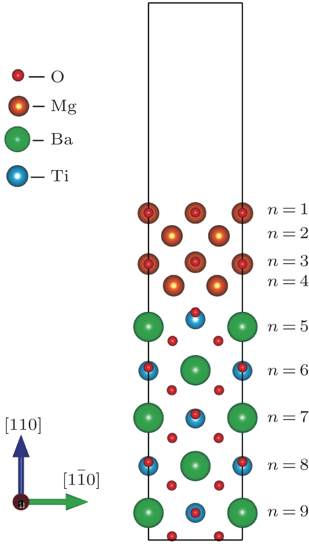
Fig. 1. Relaxed structure of the (MgO)8/(BaTiO3)5 (110) heterostructure with an n-type (MgO)0/(BaTiO)4 + interface, containing 8 unit cells (four layers) of MgO and 5 unit cells of BaTiO3 within the heterostructure. Index n denotes atomic monolayers and is increasing with the distance from the surface.
Table 1.
Table 1.
Table 1. Relative displacements between relaxed M (M denotes Ba, Ti, or Mg) and O atoms, Δ (M– O). The relative displacement denotes the displacement of cations (Ba, Ti or Mg) minus that of O anions in each layer along the c axis.
Layer n
1
2
3
4
5
6
7
8
9
Δ (Ba– O)/Å
−
−
−
−
− 0.60
− 0.17
− 0.22
− 0.24
0.00
Δ (Ti– O)/Å
−
−
−
−
− 0.42
− 0.19
− 0.26
− 0.22
0.00
Δ (Mg– O)/Å
− 0.03
0.10
0.03
0.16
−
−
−
−
−
Table 1. Relative displacements between relaxed M (M denotes Ba, Ti, or Mg) and O atoms, Δ (M– O). The relative displacement denotes the displacement of cations (Ba, Ti or Mg) minus that of O anions in each layer along the c axis.
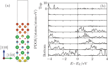
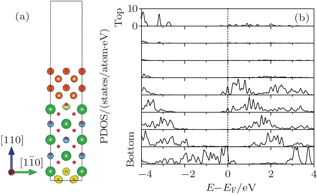
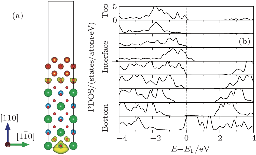
Fig. 2. (a) The 3D isovalue surface (yellow contour) of the local density of states contributing to the peak at the Fermi level. (b) The partial density of states grouped by layers of the (MgO)8/(BaTiO3)5 (110) heterostructure with an n-type interface. The data (plot of a charge isosurface and PDOS) for each layer are aligned on the same vertical position. The Fermi level is highlighted by the black dashed line.
Electronic properties of the n-type MgO/BaTiO (110) interface are calculated by the LDA method, and shown in Fig. 2. Figure 2(a) is the plot of the 3D isovalue surface (yellow contour) of the local density of states contributing to the peak at the Fermi level, which describes the spatial distribution of transferred electrons and holes, respectively. From the figure, it can be observed that the holes are confined in the bottom layer, while the free electrons concentrate preferentially at the interfaces, resulting in a 2DEG formed at the interface BaTiO layer. In order to gain more insight into the spatial distribution of electronic states, the partial density of states grouped by layers of the heterostructure is shown in Fig. 2(b). From the figure, we can see that there is a band-bending in the partial density of states. The bottom of the conduction band is determined by the Ti 3dxy band at the interface BaTiO layer, while the top of the valence band is fixed by the O 2p band in the bottom layer. Thus, the closing of the gap is due to the reducing of the interface Ti 3dxy band states at the interface BaTiO layer as the BaTiO3 slab gets thicker. With the interface Ti 3dxy electrons dipping below the Fermi level, a 2DEG emerges at the interface. Similar to the previous theoretical studies, [39– 41] it can be explained by the electronic reconstruction resulting from the polar discontinuity at the interface.
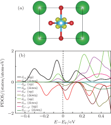
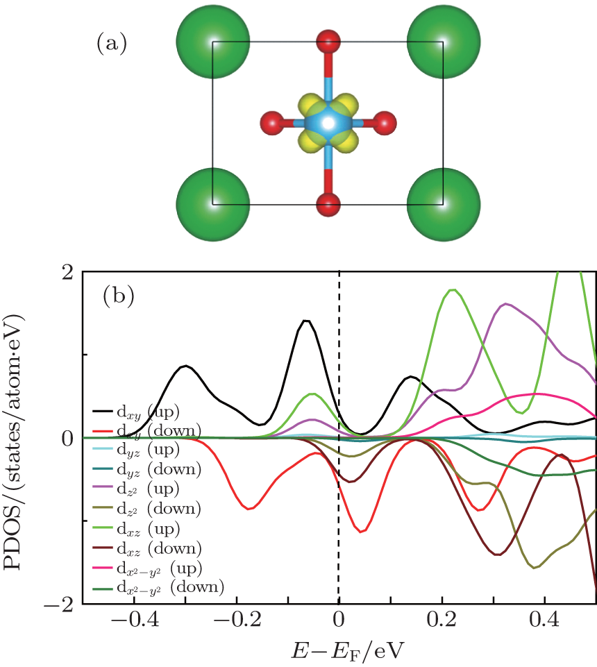
Fig. 3. (a) The spatial distributions of free electrons (yellow contour) of the interface Ti atom; this is the top view of the interface in Fig. 2(a). (b) The PDOS of the interface Ti 3d states.
To investigate the composition of the interfacial 2DEG, the spatial distributions of free electrons (yellow contour) of the interface Ti atom are shown in Fig. 3(a), which is the top view of the interface in Fig. 2(a). We can see that the 2DEG formed at the interface is dominantly composed of the interface Ti 3dxy state, and it can be confirmed by the partial density of states (PDOS) of the interface Ti 3d states, which is shown in Fig. 3(b). From Fig. 3(b), we can see that there is a large splitting of the interface Ti 3d states. This could be explained by the asymmetry at the interface: two O atoms on one side, and two Mg and two O atoms on the other side of the interface Ti atom. The Ti 3dxy state splits off from other 3d states by about 0.3 eV. The lowest dxy and higher orbitals are partly filled, thereby forming a 2DEG. From Fig. 3(b), it can also be seen that there is an unbalance between the spin-up and spin-down states, resulting in a magnetic moment of about 0.15μ B on the Ti atom of the interface. Thus the Ti 3d states, especially the lowest dxy state at the interface, contribute greatly to the metallic and magnetic properties of the n-type MgO/BaTiO (110) interface.
The polar (MgO)0/(BaTiO)4 + interface is similar to the (LaO)+ /(TiO2)0 interface in n-type LaAlO3/SrTiO3 heterostructures. This polar discontinuity creates an internal electric field in BaTiO3 and thus an increased electric potential across the BaTiO3 layers. It is similar to that which occurred in the LaAlO3 slab of the LaAlO3/SrTiO3 heterostructure. In the LaAlO3/SrTiO3 heterostructure, the interface becomes metallic when the LaAlO3 slab thickness is above 4 unit cells.[5, 6] Here, we vary the thickness of BaTiO3 to search for the critical thickness of the metallic BaTiO3/MgO (110) interface.
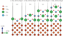
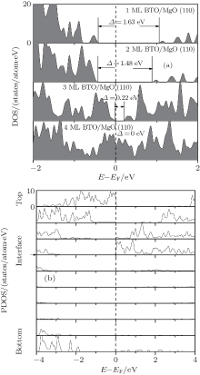
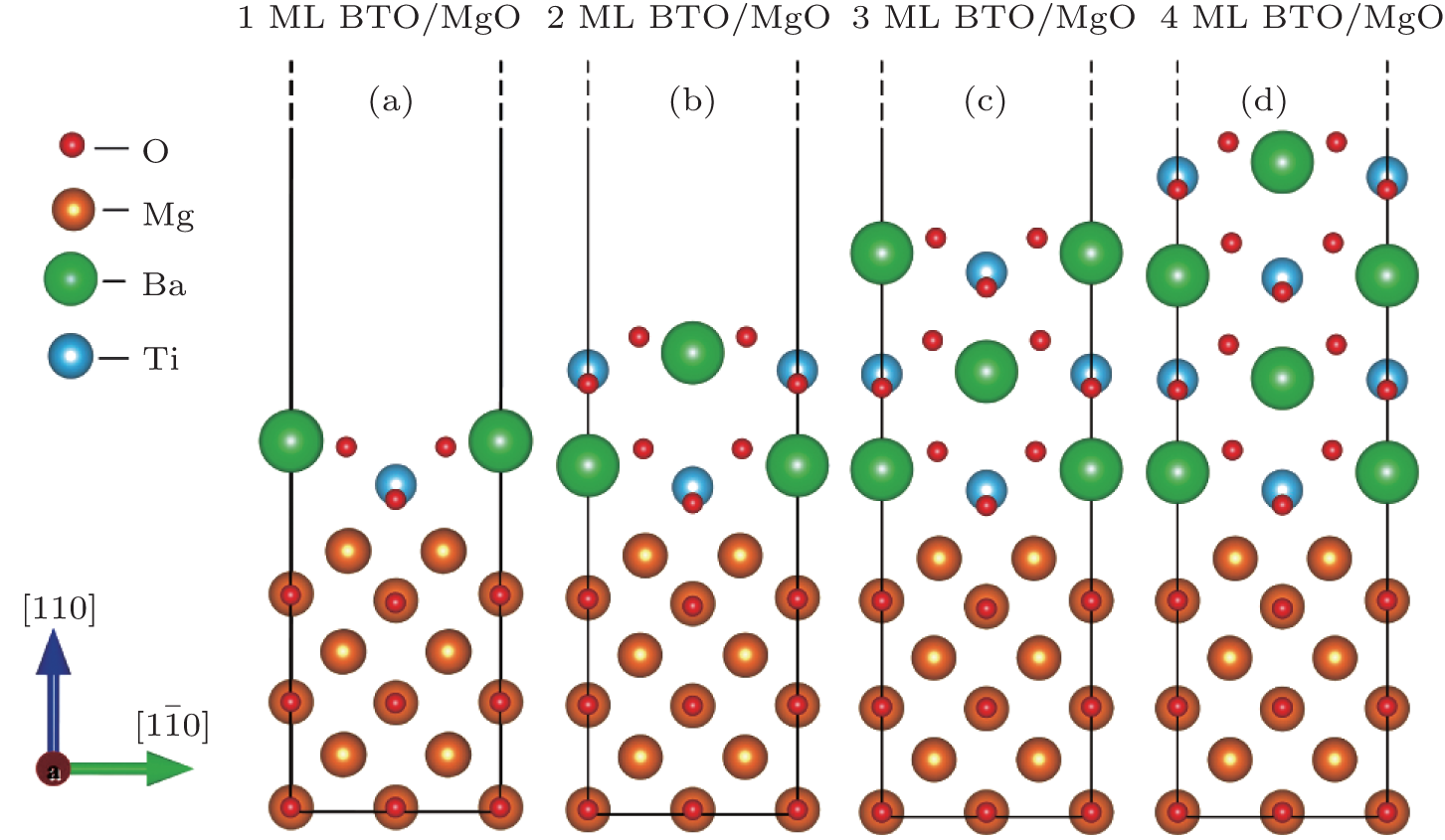
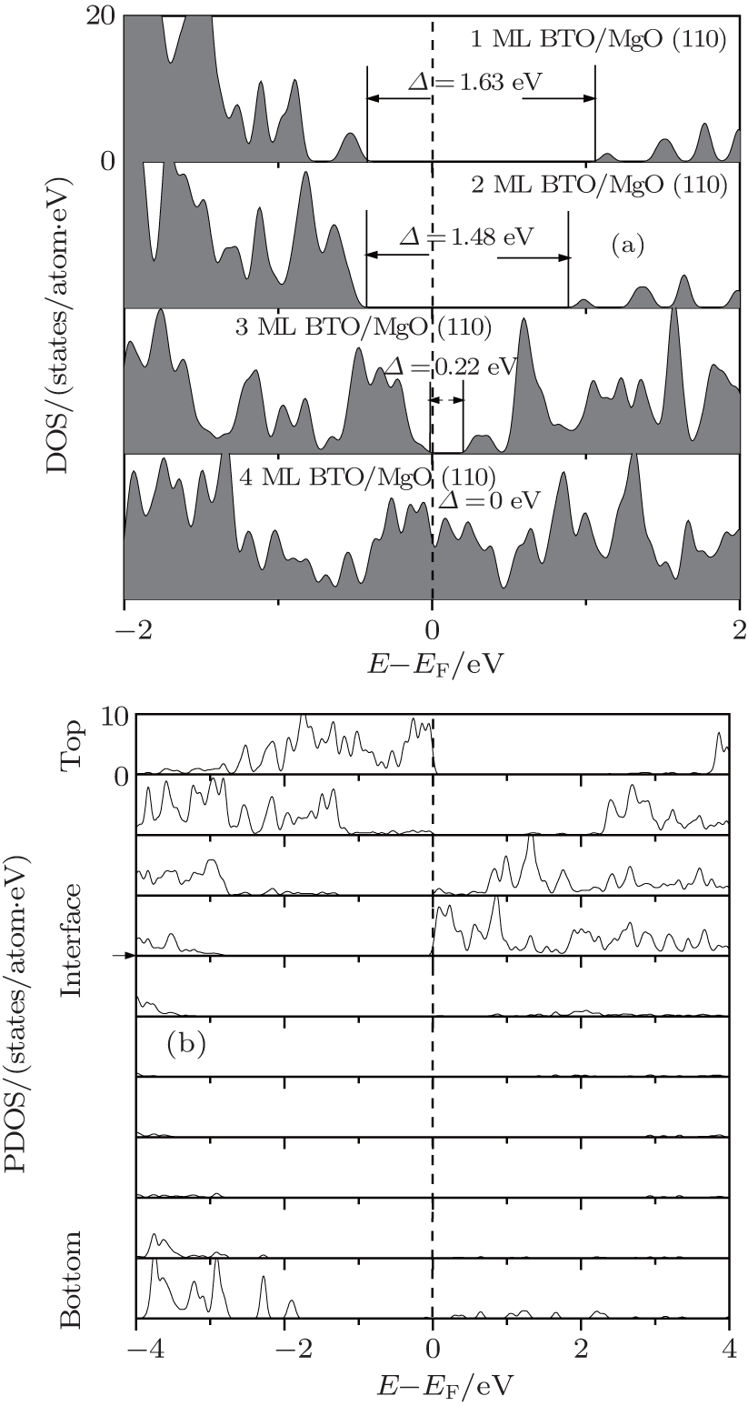
Relaxed 1– 4 ML thick BaTiO3 films on MgO (110) are shown in Fig. 4. From the figure, we can see that the relaxation of the MgO slab is unconspicuous in the four models. In contrast, the displacements of atoms in the BaTiO3 slab are significant: Ti and Ba atoms relax away from the interface while O atoms relax close to the interface. It is similar to that in the MgO/BaTiO (110) interface. The total density of states as a function of the BaTiO3 thickness for 1– 4 ML thick BaTiO3 films on MgO (110) is shown in Fig. 5(a). With increasing thickness of the BaTiO3 film, the band gap decreases from 1.63 eV for 1 ML BaTiO3 and finally closes for 4 ML BaTiO/MgO (110). The results predict an insulator-to-metal transition. In order to gain more insight into the type of electronic states around the Fermi level and their spatial distribution, the layer-resolved density of states for the 4 ML BaTiO/MgO (110) is calculated, and plotted in Fig. 5(b). From the figure, a nearly rigid upward shift of the O 2p bands towards the Fermi level is observed as they approach the surface. For the relaxed BaTiO/MgO (110) heterostructure, the top of the valence band is determined by the O 2p states in the surface O2 layer, while the bottom of the conduction band is determined by the Ti 3d states at the interface. Thus, the closing of the gap is due to the raising of the O 2p states in the surface O2 layer and the reducing of the Ti 3d states at the interface as the BaTiO3 slab gets thicker. Once the BaTiO3 slab thickness is above 4 unit cells, the BaTiO/MgO (110) interface becomes metallic, and a 2DEG is formed at the interface.
Fig. 4. Relaxed (a) 1 ML, (b) 2 ML, (c) 3 ML, and (d) 4 ML thick BaTiO3 films on MgO (110).
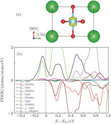
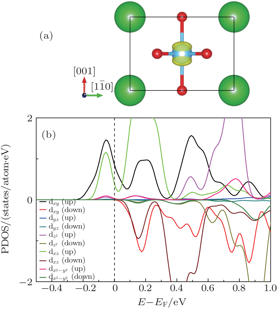
MgO grown on a BaTiO3 substrate is under compressive stress, while BaTiO3 grown on a MgO substrate is under tensile stress. The different interface stress may influence the formation of the 2DEG. To investigate the composition of the 2DEG formed at the BaTiO/MgO (110) interface, the 3D isovalue surface (yellow contour) of the local density of states of the interface Ti atom for 5 ML BaTiO/MgO (110) is calculated, and shown in Fig. 6(a). From the figure, we can see that the 2DEG formed at the interface is dominantly composed of interface Ti 3dxy and 3dxz orbitals, and it can be confirmed by the PDOS of the interface Ti 3d states, which is shown in Fig. 6(b). From the figure, we can see that there is a large splitting of the interface Ti 3d states: the Ti 3dxy state splits off from other 3d states by about 0.1 eV. The lowest dxy and higher orbitals are partly filled, thereby forming a 2DEG. In addition, from Fig. 6(b), it can also be seen that there is an unbalance between the spin-up and spin-down states, resulting in a magnetic moment of about 0.20μ B on the Ti atom of the interface. Comparing Fig. 6 with Fig. 3, it can be found that the occupation and splitting of the interface Ti 3d states are different. It suggests that the interface stress plays an important role in the composition of the 2DEG.
Fig. 5. (a) The total density of states as a function of the BaTiO3 thickness for 1– 4 ML thick BaTiO3 films on MgO (110). (b) The layer-resolved density of states for 4 ML BaTiO/MgO (110).
Fig. 6. (a) The 3D isovalue surface (yellow contour) of the local density of states of the interface Ti atom contributing to the peak at the Fermi level. (b) The partial density of states (PDOS) of the interface Ti 3d states.
3.2 The p-type interface
Figure 7 shows the relaxed p-type MgO/O2 (110) interface. From the figure, we can see that the relaxation of the BaTiO3 slab is more obvious than that of the MgO slab. In addition, it can be seen that both Ti and Ba atoms relax close to the interface, while all O atoms relax away from the interface. A more thorough insight can be obtained by analyzing the relative displacements between M (M denotes Ba, Ti or Mg) and O atoms, which are listed in Table 2. From the table, we can see that the largest structural relaxation occurs in the interface BaTiO layer. In the layer, the relative displacement between O and Ba atoms results in a big buckling of 0.40 Å . The relative displacement between O and Ti (Ba) ions results in a polarization P pointed to the interface, which can reduce the built-in potential in the BaTiO3 (110) slab and the instability of the polar interface.
Fig. 7. Relaxed structure of the (MgO)8/(BaTiO3)5 (110) heterostructure with a p-type (MgO)0/(O2)4 − interface, containing 8 unit cells (four layers) of MgO and 5 unit cells of BaTiO3 within the heterostructure. Index n denotes atomic monolayers and is increasing with the distance from the surface.
Figure 8 displays the electronic properties of the p-type MgO/O2 (110) interface. Figure 8(a) shows the 3D isovalue surface (yellow contour) of the local density of states contributing to the peak at the Fermi level, which describes the spatial distribution of transferred electrons and holes. From the figure, it can be observed that the electrons are confined in the bottom layer, while the holes are confined at the interface MgO layer. In order to gain more insight into the spatial distribution of electronic states, the partial density of states grouped by layers of the heterostructure is shown in Fig. 8(b). Owing to the polar structure of BaTiO3 along the [110] direction, the electric field through the BaTiO3 film lifts up the valence band edge and reduces the band gap. When the interface O 2py state surpasses the Fermi level, a conducting interface emerges. It can also be explained by the electronic reconstruction resulting from the polar discontinuity at the interface.
Table 2.
Table 2.
Table 2. Relative displacements between relaxed M (M denotes Ba, Ti or Mg) and O atoms Δ (M– O). The relative displacement denotes the displacement of cations (Ba, Ti or Mg) minus that of O anions in each layer along the c axis.
Layer n
1
2
3
4
5
6
7
8
9
Δ (Ba– O)/Å
−
−
−
−
0.40
0.18
0.23
0.27
0.00
Δ (Ti– O)/Å
−
−
−
−
0.29
0.26
0.26
0.30
0.00
Δ (Mg– O)/Å
− 0.10
− 0.06
− 0.06
− 0.16
−
−
−
−
−
Table 2. Relative displacements between relaxed M (M denotes Ba, Ti or Mg) and O atoms Δ (M– O). The relative displacement denotes the displacement of cations (Ba, Ti or Mg) minus that of O anions in each layer along the c axis.
Fig. 8. (a) The 3D isovalue surface (yellow contour) of the local density of states contributing to the peak at the Fermi level. (b) The partial density of states grouped by layers of the (MgO)8/(BaTiO3)5 (110) heterostructure with a p-type interface. The data (plot of a charge isosurface and PDOS) for each layer are aligned on the same vertical position. The Fermi level is highlighted by the black dashed line.
Fig. 9. (a) The 3D isovalue surface (yellow contour) of the local density of states of the interface MgO layer contributing to the peak at the Fermi level, and it is the top view of the interface in Fig. 8(a). (b) The PDOS of the O 2p states in the interface MgO layer.
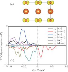
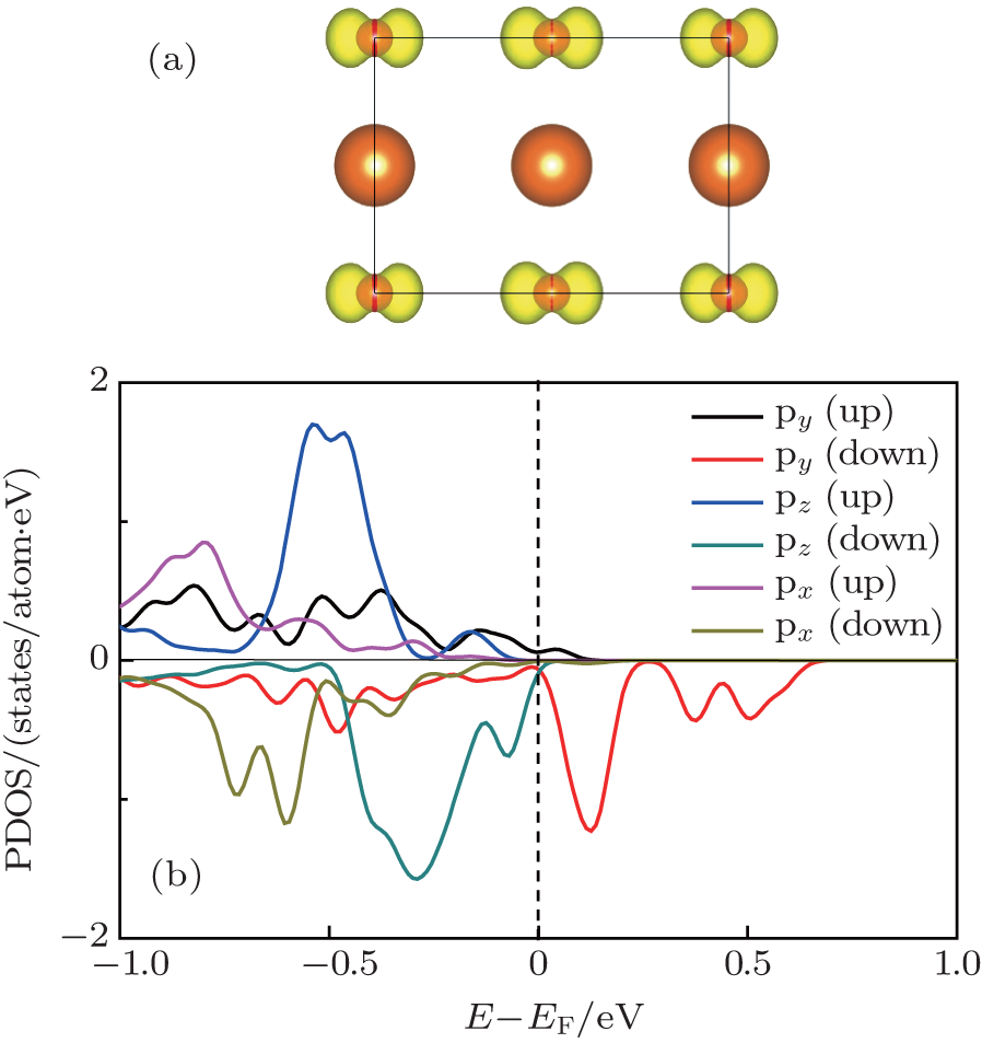
To investigate the composition of the interfacial holes, the 3D isovalue surface (yellow contour) of the local density of states of the interface MgO layer contributing to the peak at the Fermi level is calculated, and shown in Fig. 9(a). From the figure, we can see that the interfacial holes dominantly come from the O 2py orbital in the interfacial MgO layer, and it can be confirmed by the PDOS of the O atoms in the interfacial MgO layer shown in Fig. 9(b). In Fig. 9(b), we can see that the interface O 2p states split and the O 2py state splits off from other O 2p states by 0.55 eV. The partly filled O 2py state contributes mainly to the formation of the interface holes. In addition, there is an unbalance between the spin-up and spin-down states, resulting in a magnetic moment of about 0.25μ B on the O atom of the interface.
4 Conclusion
The results of first-principles calculations clearly demonstrate that other polar interfaces, besides LaAlO3/SrTiO3, can show a two-dimensional metallic behavior. Based on the analyses of the electronic properties of the n-type polar interfaces, it can be seen that the interface Ti 3d states contribute greatly to the metallic and magnetic properties. Varying the thickness of BaTiO3 may induce a metal– insulator transition. Once the BaTiO3 slab thickness is above 4 unit cells, the n-type interface becomes metallic. For the p-type polar interface, holes preferentially occupy the interface O 2py state, resulting in a conducting interface. The unbalance of the spin splitting of the O 2p states in the interface MgO layer leads to a magnetic moment of about 0.25 μ B per O atom at the interface. All these results add to the understanding of these polar interfaces and further suggest that interface engineering is an attractive and useful approach to creating novel properties in correlated electron systems.
KalabukhovA, GunnarssonR, BörjessonJ, OlssonE, ClaesonT and WinklerD2007Phys. Rev. B75121404DOI:10.1103/PhysRevB.75.121404[Cited within:1]
3
SiemonsW, KosterG, YamamotoH, HarrisonW A, LucovskyG, GeballeT H, BlankD H A and BeasleyM R2007Phys. Rev. Lett. 98196802DOI:10.1103/PhysRevLett.98.196802[Cited within:1][JCR: 7.943]
4
MauriceJ L, HerranzG, ColliexC, DevosI, CarrétéroC, BarthélémyA, BouzehouaneK, FusilS, ImhoffD, JacquetE, JomardF, BallutaudD and BasleticM2008Europhys. Lett. 8217003DOI:10.1209/0295-5075/82/17003[Cited within:1][JCR: 2.26]
5
HuijbenM, RijndersG, BlankD H A, BalsS, AertS V, VerbeeckJ, TendelooG V, BrinkmanA and HilgenkampH2006Nat. Mater. 5556DOI:10.1038/nmat1675[Cited within:2][JCR: 35.749]
6
BellC, HarashimaS, HikitaY and HwangH Y2009Appl. Phys. Lett. 94222111DOI:10.1063/1.3149695[Cited within:2][JCR: 3.794]
BarkC W, FelkerD A, WangY, ZhangY, JangH W, FolkmanC M, ParkJ W, BaekS H, ZhouH, FongD D, PanX Q, TsymbalE Y, RzchowskiM S and EomC B2011Proceedings of the National Academy of Sciences1084720[Cited within:1]
VerbeeckJ, BalsS, KravtsovaA N, LamoenD, LuysbergM, HuijbenM, RijndersG, BrinkmanA, HilgenkampH, BlankD H A and TendelooG V2010Phys. Rev. B81085113DOI:10.1103/PhysRevB.81.085113[Cited within:1]
14
WangH Y, DuanZ G, LiaoW H and ZhouG H2010Chin. Phys. B19142049DOI:10.1088/1674-1056/19/3/142049[Cited within:1][JCR: 1.148][CJCR: 1.2429]
15
DuY L, WangC L, LiJ C, XuP P, ZhangX H, LiuJ, SuW B and MeiL M2014Chin. Phys. B23087302DOI:10.1088/1674-1056/23/8/087302[Cited within:1][JCR: 1.148][CJCR: 1.2429]
... IntroductionSince a high-mobility electron gas was discovered at the LaAlO3/SrTiO3 interface,[1] much effort has been devoted to reveal its origin ...
... [1,11#cod#x2013 ...
1
2007
0.0
0.0
... Many researchers have investigated the roles of many factors, including oxygen vacancies,[2,3] chemical intermixing,[4] the thickness of the LaAlO3 sheets,[5,6] the external#cod#x00A0 ...
1
2007
7.943
0.0
... Many researchers have investigated the roles of many factors, including oxygen vacancies,[2,3] chemical intermixing,[4] the thickness of the LaAlO3 sheets,[5,6] the external#cod#x00A0 ...
1
2008
2.26
0.0
... Many researchers have investigated the roles of many factors, including oxygen vacancies,[2,3] chemical intermixing,[4] the thickness of the LaAlO3 sheets,[5,6] the external#cod#x00A0 ...
2
2006
35.749
0.0
... Many researchers have investigated the roles of many factors, including oxygen vacancies,[2,3] chemical intermixing,[4] the thickness of the LaAlO3 sheets,[5,6] the external#cod#x00A0 ...
... [5,6] Here, we vary the thickness of BaTiO3 to search for the critical thickness of the metallic#cod#x00A0 ...
2
2009
3.794
0.0
... Many researchers have investigated the roles of many factors, including oxygen vacancies,[2,3] chemical intermixing,[4] the thickness of the LaAlO3 sheets,[5,6] the external#cod#x00A0 ...
... [5,6] Here, we vary the thickness of BaTiO3 to search for the critical thickness of the metallic#cod#x00A0 ...
1
2006
0.0
0.0
... electric field,[7#cod#x2013 ...
1
2008
38.597
0.0
1
2011
5.008
0.0
... 9] and the epitaxial strain ...
1
2011
0.0
0.0
... [10] Besides them, the polarity discontinuity at the interface has been considered to be the dominant mechanism behind the phenomenon ...
1
2006
0.0
0.0
... [1,11#cod#x2013 ...
1
2006
0.0
0.0
1
2010
0.0
0.0
1
2010
1.148
1.2429
1
2014
1.148
1.2429
... 15] In LaAlO3/SrTiO3(001) heterostructures, the atomic layers in SrTiO3 are nominally charge neutral, whereas the atomic layers in LaAlO3 can be represented by alternating (LaO)#cod#x002B ...
1
2006
35.749
0.0
... [16] ...
2
2007
7.943
0.0
... [17#cod#x2013 ...
... 19] Hotta and his cooperator[17] investigated the transport properties of LaVO3/SrTiO3 heterointerfaces, and found that the n-type VO2/LaO/TiO2 interface is conducting, while the p-type VO2/SrO/TiO2 interface is insulating, similar to that in LaAlO3/SrTiO3 ...
1
2009
0.0
0.0
... [18] studied the LaAlO3/EuO(001) interface, and demonstrated that the mechanism responsible for the two-dimensional electron gas (2DEG) at the interface is similar to that for the LaAlO3/SrTiO3 interface ...
2
2010
3.794
0.0
... 19] Hotta and his cooperator[17] investigated the transport properties of LaVO3/SrTiO3 heterointerfaces, and found that the n-type VO2/LaO/TiO2 interface is conducting, while the p-type VO2/SrO/TiO2 interface is insulating, similar to that in LaAlO3/SrTiO3 ...
... [19] investigated heterostructures based on a different overlayer ...
2
1975
0.0
0.9894
... ,[20] while the lattice constant of BaTiO3 with the perovskite cubic structure is 4 ...
... [20,32] Thus, to modulate the thin layers of BaTiO3 grown on the top of the MgO substrate, the in-plane lattice constants a and b of the heterostructures are fixed at 4 ...
The correlation ([ ` ( a )] 2 + [ ` ( a )] 3 ) = ([ ` ( a )] 1 + [ ` ( a )] 4 ) (\bar a_2 + \bar a_3 ) = (\bar a_1 + \bar a_4 ) has been established for the mean parameters of the reduced perovskite unit cells, [ ` ( a )] 1 ,[ ` ( a )] 2 ,[ ` ( a )] 3 \bar a_1 ,\bar a_2 ,\bar a_3 and [ ` ( a )] 4 \bar a_4 of four arbitrary compounds with the perovskite structure having the compositions (1) ABX 3 , (2) A′BX 3 , (3) AB′X 3 , and (4) A′B′X 3 , where A, A′ and B, B′ are the pairs of metal atoms with equal valences and X is an oxygen or halogen atom. The above correlation is consistent with the model of harmonic quasi-elastic atomic interactions.
1.Rostov State University Institute of Physics pr. Stachki 194 Rostov-on-Don 344090 Russia pr. Stachki 194 Rostov-on-Don 344090 Russia
... ,[21] so there is a little lattice mismatch between MgO and BaTiO3 ...
... [21] and other theoretical results of 3 ...
1
2004
3.794
0.0
... Due to its broad applications in capacitors[22] and electro-optical devices,[23,24]BaTiO3/MgO (001) has attracted much attention, and been fabricated using magnetron sputtering,[25#cod#x2013 ...
2
2002
3.794
0.0
... Due to its broad applications in capacitors[22] and electro-optical devices,[23,24]BaTiO3/MgO (001) has attracted much attention, and been fabricated using magnetron sputtering,[25#cod#x2013 ...
... [23,29] However, there are few studies about the polar MgO/BaTiO3 (110) interfaces ...
1
1998
0.0
0.0
... Due to its broad applications in capacitors[22] and electro-optical devices,[23,24]BaTiO3/MgO (001) has attracted much attention, and been fabricated using magnetron sputtering,[25#cod#x2013 ...
1
1995
0.71
0.0
... Due to its broad applications in capacitors[22] and electro-optical devices,[23,24]BaTiO3/MgO (001) has attracted much attention, and been fabricated using magnetron sputtering,[25#cod#x2013 ...
In this paper, BaTiO 3 thin films were prepared by RF magnetron sputtering on MgO substrates and their properties such as the crystal structure and optical waveguide properties were investigated. The optimum deposition parameters, such as substrate temperature, deposition pressure, gas flow ratio, the RF power and the after annealing temperature, were obtained in order to get the best BaTiO 3 film quality. The XRD results show that highly c -axis textured BaTiO 3 thin films were successfully grown on MgO substrate. Films obtained under the optimum deposition parameters, substrate temperature of 650°C, RF power of 50 W, deposition pressure 18 mTorr and gas flow ratio O 2 /(Ar+ O 2 ) of 15% namely, reaches a full width at half maximum intensity (FWHM) of BaTiO 3 (002) XRD peak of 0.25°. The FWHM of BaTiO 3 (002) XRD peak was further reduced to 0.24° via post-treatment with furnace annealing (at 800°C for 2 h) which indicates the film crystal quality is further improved. The bright and sharp TE modes measured by m-line spectroscopy of the BaTiO 3 film were observed indicating its possible application in optical waveguide.
1.Tatung University Graduate Institute in Electro-Optical Engineering No. 40, Sec. 3, Chungshan North Road Taipei 104 Taiwan, ROC
Conductive (La0.5Sr0.5)CoO3 and Pt layers were prepared on (100)MgO substrate respectively as bottom electrode for BaTiO3 films. While the (La0.5Sr0.5)CoO3 layer showed a cube-on-cube epitaxy on MgO, thus promoting the heteroepitaxial growth of the successively grown BaTiO3 film, the Pt layer was polycrystalline with a texture highly dependent on the growth temperature. BaTiO3 films of the same thickness (similar to 320 nm) deposited on (La0.5Sr0.5)CoO3 and Pt layers with different textures were comparatively investigated. The differences in electrical properties are found to be closely related to the crystalline orientation and interface states of the BaTiO3 films on different bottom electrode layers. (C) 2013 Elsevier B.V. All rights reserved.
The crystal structure of BaTiO 3 thin films grown by pulsed laser deposition on MgO substrates was found to be strongly influenced by the oxygen pressure used during growth. Low pressures produced epitaxial films with highly strained out-of-plane lattice parameter c compared to in-plane parameter a , while increasing oxygen pressure resulted in the ratio c / a c / a c / a c -oriented films. Moderate shifts in oxygen working pressure were demonstrated to produce films with very different properties thereby offering convenient means for strain engineering and control of preferred crystal orientation and polarization direction of highly oriented BTO films.
1.Massachusetts Institute of Technology Department of Materials Science and Engineering 77 Massachusetts Avenue Cambridge MA 02139 USA 2.Technical Research Centre of Finland Kaitovayla 1 90571 Oulu Finland 3.University of Oulu Microelectronics and Materials Physics Laboratory P.O. Box 4500 90014 Oulu Finland
... [23,29] However, there are few studies about the polar MgO/BaTiO3 (110) interfaces ...
1
2004
0.0
0.0
... [30] and 3 ...
1
2008
0.0
0.0
... [31] Thus, the in-plane lattice constants a and b of the heterostructures are fixed at 3 ...
1
2011
1.317
0.2214
... [20,32] Thus, to modulate the thin layers of BaTiO3 grown on the top of the MgO substrate, the in-plane lattice constants a and b of the heterostructures are fixed at 4 ...
1
1996
0.0
0.0
... [33,34] The ion#cod#x2013 ...
1
1999
0.0
0.0
... [33,34] The ion#cod#x2013 ...
1
1994
0.0
0.0
... electron interactions are described by using the projector augmented wave (PAW) method,[35] and the local density approximation (LDA) is used for the exchange#cod#x2013 ...
1
1980
7.943
0.0
... [36] Calculations are performed using a 5#cod#x00D7 ...
1
1976
0.0
0.0
... Pack[37]k-point mesh and a kinetic energy cutoff of 500#cod#x00A0 ...
1
2014
0.0
0.0
... relative displacement between O and Ti (Ba) ions results in a polarization P pointed away from the interface, which can reduce the built-in potential in the BaTiO3 (110) slab[38] and the instability of the polar interface ...
1
2007
7.943
0.0
... Similar to the previous theoretical studies,[39#cod#x2013 ...
1
2010
0.0
0.0
1
2009
7.943
0.0
... 41] it can be explained by the electronic reconstruction resulting from the polar discontinuity at the interface ...
Two-dimensional metallic behavior at polar MgO/BaTiO3 (110) interfaces*
[Du Yan-Linga),b), Wang Chun-Leia), Li Ji-Chaoa)†, Zhang Xin-Huaa), Wang Fu-Ninga), Liu Jiana), Zhu Yuan-Hua), Yin Naa), Mei Liang-Moa)]


 , Zhang Xin-Hua