


New SOI power device with multi-region high-concentration fixed interface charge and the model of breakdown voltage*
[Li Qia), b) , Li Hai-Oua)†  , Tang Ning
a) , Zhai Jiang-Huia) , Song Shu-Xiangc) ]
, Tang Ning|
|


†Corresponding author. E-mail: lqmoon@guet.edu.cn
Project supported by the State Key Laboratory of Electronic Thin Films and Integrated Devices of China (Grant No. KFJJ201205), the Department of Education Project of Guangxi Province, China (Grant No. 201202ZD041), the Postdoctoral Science Foundation Project of China (Grant Nos. 2012M521127 and 2013T60566), and the National Natural Science Foundation of China (Grant Nos. 61361011, 61274077, and 61464003).
A new SOI power device with multi-region high-concentration fixed charge (MHFC) is reported. The MHFC is formed through implanting Cs or I ion into the buried oxide layer (BOX), by which the high-concentration dynamic electrons and holes are induced at the top and bottom interfaces of BOX. The inversion holes can enhance the vertical electric field and raise the breakdown voltage since the drain bias is mainly generated from the BOX. A model of breakdown voltage is developed, from which the optimal spacing has also been obtained. The numerical results indicate that the breakdown voltage of device proposed is increased by 287% in comparison to that of conventional LDMOS.
The lateral double diffused MOS transistor (LDMOS) has been widely used in intelligent power applications by virtue of the advantage of the process which is compatible to a very large integration process and is easy to integrate with low-voltage devices.[1, 2] Moreover, if a silicon-on-insulator (SOI) technology is used, low leakage current, high breakdown voltage (BV), and low specific on-resistance are also achieved.[3, 4] In order to be feasibly isolated from low-voltage devices, LDMOS needs a thin layer and satisfies the reduced surface field (RESURF) principle.[5, 6] However, in order to obtain high BV, the thickness of buried oxide layer (BOX) should be increased, which causes self-heating effects; different structures have therefore been proposed to overcome this trade-off.[7– 10]
Introducing the fixed charge in the buried oxide is an effective way to increase the electric field of dielectric layer and improve the vertical BV, [4, 8] but it is very difficult to fabricate for many masks to form linear profile of fixed charge. In this letter, a novel LDMOS high-concentration multi-region fixed charge (MHFC) is proposed for the first time. The MHFC at interface of buried oxide is employed to enhance the vertical electric field in BOX and obtain high BV and low on-resistance due to the transfer of major portion of reverse bias from Si to BOX, which has advantages of high tolerance of technology process and allowance of high temperature. A model of BV is also presented to optimize the proposed device.
The schematic cross-section of the MHFC device is illustrated in Fig. 1(a), which is featured by substantial uniformly-spaced high-concentration fixed positive charge at the interface of BOX, compared to the cross-section of conventional device in Fig. 1(b).
The doping concentration of the drift region is Nd and its length is equal to Ld. td and tox are the thicknesses of drift region and BOX, respectively. x and y are the horizontal and vertical positions, respectively. tp and Np are the thickness and doping concentration of the surface P-type region. The width and distance of fixed charge region are W and D, respectively. σ f is the concentration of fixed charge and is always above 1× 1013 cm– 2. The MHFC LDMOS can be fabricated using the MOS process in the SOI substrate, in which the BOX is implanted with I, B, or Cs ion to form the MHFC.
When the positive voltage Vd biased to the N+ Nd junction, the whole drift region is completely depleted. Divide the drift region into n regions as shown in Fig. 1(a) (n is the number of MHFC cells), supposing equal charge density in each MHFC cell. The potential function φ i (x, y) in the drift region follows the 2D Poisson equation, and the boundary conditions are given by

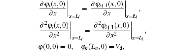
where ɛ ox and ɛ si are the dielectric constant of oxide layer and silicon, respectively.
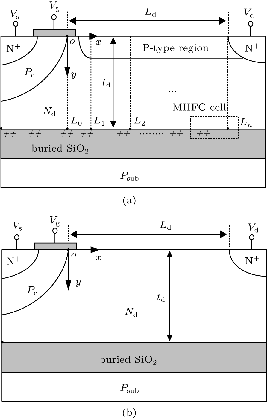 | Fig. 1. (a) Cross-section of MHFC LDMOS; (b) cross-section of conventional LDMOS. |
Solving the 2D Poisson equation with the vertical electric field Ey(Ld, y) along x = Ld in every region, the lateral surface electric Ex (x, 0) is expressed as


where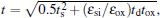
Figure 2(a) shows the distribution of the dynamic interface charges (y = 4.9 μ m) at Vd = BV, and it can be seen that there are plenty of electrons right over the top interface of each high-concentration positive fixed charge region which is almost the same and equals ∼ 1× 1019 cm-3. High levels of holes are induced by electrons and increase from 2× 1018 cm-3 for source to 9× 1018 cm-3 for drain. From Eq. (5), interface charges (holes) will lead to a considerable increase of EI. Due to absence of interface charges in conventional LDMOS, the electric field ESi of Si layer rapidly reaches the silicon critical electric field of about 30 V/μ m and EI is always limited to 90 V/μ m. Thanks to the increase of the self-adaptive holes introduced by fixed charges in BOX, the EI in the MHFC device is continuously enhanced, and ESi is simultaneously reduced, which makes the major portion of bias sustained by BOX and leads to the increase of BV. Figures 2(b) and 2(c) show the equipotential contours and the distributions of the surface electric field at breakdown, and both surface electric fields are effectively optimized according to the RESURF principle. Because of the electric field modulation by dynamic electrons and holes in BOX, the equipotential contour of MHFC SOI is much more uniform, which results in a higher BV for MHFC LDMOS (597 V) than conventional LDMOS (208 V). Figure 2(d) shows the vertical electric field and potential, and the analytic results are in good agreement with the numerical results. As a result of the shielding effect of electric field by dynamic holes between the fixed charge regions, the vertical electric field of MHFC reaches 5.9× 10⁶ V/cm, much higher than 0.95× 10⁶ V/cm. The voltage sustained by the BOX is above 90% of drain bias in MHFC, leading to a full exploitation of breakdown characteristic of buried oxide layer. The parameters of structure are: (i) for conventional device, Nd = 2.8× 1015 cm-3, td = 5 μ m, Ld = 55 μ m, tox = 1 μ m; (ii) for MHFC device, tp = 1 μ m, Np = 1.5× 1016 cm-3, σ f = 1× 1013 cm-2, Nd = 2.8× 1015 cm-3, td = 5 μ m, Ld = 55 μ m, and W = D = 1 μ m.
 | Fig. 2. Surface electric field, potential and charge distributions. (a) Dynamic electron and hole profile of buried oxide layer in MHFC. (b) Equipotential contour of MHFC. (c) Surface electric field distribution of MHFC and conventional device. (d) Vertical electric field and potential distribution. |
As seen in Fig. 3(a), the optimal Nd decreases with the increase in td. The maximum BV increases slightly with augmentation of td for only a small portion of vertical voltage is generated by the Si layer. For the same 5 μ m of td, the BV of MHFC is three times larger than that of a conventional LDMOS by virtue of the introduction of a high-concentration fixed charge and enhancement of electric field in the BOX. The influences of Nd on the BV are shown in Fig. 3.
In Fig. 3(b), the maximum BV increases with the rise of tox because more voltage is sustained by the BOX. The higher the thickness tox is, the weaker the modulation of vertical electric field on drift region, so optimum Nd decreases. Nd is typically inversely proportional to td in order to guarantee that the drift region is depleted fully and obtain high BV.
 | Fig. 3. Influence of Nd on the BV with (a) different td and (b) different tox, and the BV has a clear optimum. |
The main effect of MHFC is to induce the dynamic interface charges including the electrons and holes. Once its concentration reaches a certain value, its influence on BV is very small. It is apparent from Fig. 4(a) that the curve is characterized by both the increase and saturation regions. In the increase region, because MHFC can attract dynamic charge at the interface of BOX, so more MHFC induces higher BV. With the increase of fixed charge concentration, the BV nearly reaches saturated value when the concentration of MHFC is increased to 1× 1013 cm-2. The saturated BV increases with increase of tbox. The optimal Nd increases with the decrease of concentration of MHFC. In Fig. 4(b), the positive dynamic holes can enhance EI and vertical BV, so BV decreases with the increase of the distance D between two adjacent high-concentration fixed charge regions. When Ld is small, the lateral breakdown happens and the BV increases with the increase of Ld. When Ld increases to a certain value, BV reaches a constant value limited by the vertical breakdown. The width W of fixed charge region has a optimal value due to the modulation effect of the electric field from dynamic charges. With the increase of tox, the optimal W decreases as shown in Fig. 4(c).
'> | Fig. 4. Influence of MHFC's parameters on (a) breakdown voltage, (b) concentration of MHFC, (c) distance between two adjacent regions of fixed charge, and (d) width of fixed charge region. |
The BV rises with the increase of tox since higher voltage is sustained by BOX (see Fig. 5(a)). With the same tox, the major portion of reverse bias is sustained by BOX in the MHFC LDMOS, so the BV increases sharply with the rise of tox. By comparison, the magnitude of electric field is small and the BV increases slowly in conventional device. A fair accordance between the analytical and numerical results may generally be found, showing the validity of the model presented. In Fig. 5(b), the optimum Nd increases with the rise of Np in order to obtain the optimal distribution of surface electric field. The maximum BVs are obtained and change little when the dose of surface P-type region is nearly the same. In the practical device design, the critical factors to BV are the width and distance of MHFC, and it is applauded to reduce on-resistance by raising Np in condition of fully depleted state.
 | Fig. 5. Dependence of BV on (a) tox and (b) Np. |
Figure 6 shows the influence of structure parameters on on-resistance. The optimal Nd increases with the increase of Np due to the charge sharing effect of drift region in Fig. 6(a). Meanwhile the specific on-resistance decreases. The effect of dynamic holes induced by fixed charge is similar to N-type charge of drift region, so the optimal Nd is equal to that of conventional device due to the fact that the surface P-type region is compensated by fixed charge region in buried oxide. When Np = 0, the optimal Nd is very small, resulting in a large on-resistance. With the same parameter, the BV of the MHFC increases from 205 V of conventional device to 597 V, but the specific on-resistance increases less than twice. With the increase of tp, the number of carriers decreases, and thus the on-resistance increases (see Fig. 6(b)).
 | Fig. 6. Dependence of BV and on-resistance on Nd with (a) different Np and (b) different tp. |
Table 1 shows characteristics of several structures. Compared to the structure with self-adaptive interface charge, [13] the conductance factor is more than doubled in the MHFC device. The conductance factor in shield trench device is less than half of the proposed device with the same BV, but it is very difficult to fabricate.[11]
| Table 1. Comparison between several structures. |
A new MHFC structure is proposed. A large number of dynamic holes are introduced by high-concentration multiple-region fixed charge, which can strengthen dramatically the vertical electric field in buried oxide layer and results in the significant improvement of BV. The analytical and simulation results have demonstrated an improvement of the trade-off between the BV and on-resistance. The MHFC is attractive for applications in thin high-voltage device and power integrated circuits for its favorable performances.
| 1 |
|
| 2 |
|
| 3 |
|
| 4 |
|
| 5 |
|
| 6 |
|
| 7 |
|
| 8 |
|
| 9 |
|
| 10 |
|
| 11 |
|
| 12 |
|
| 13 |
|