
Spin and valley filter in strain engineered silicene
[Wang Sa-Ke, Wang Jun† ]
]
]
 |


†Corresponding author. E-mail: jwang@seu.edu.cn
The realization of a perfect spin or valley filtering effect in two-dimensional graphene-like materials is one of the fundamental objectives in spintronics and valleytronics. For this purpose, we study spin- and valley-dependent transport in a silicene system with spatially alternative strains. It is found that due to the valley-opposite gauge field induced by the strain, the strained silicene with a superlattice structure exhibits an angle-resolved valley and spin filtering effect when the spin–orbit interaction is considered. When the interaction that breaks the time reversal symmetry is introduced, such as the spin or valley dependent staggered magnetization, the system is shown to be a perfect spin and valley half metal in which only one spin and valley species is allowed to transport. Our findings are helpful to design both spintronic and valleytronic devices based on silicene.
Silicene is a two-dimensional (2D) graphene-like material that has been successfully synthesized in the laboratory recently.[1, 2] Compared to graphene, silicene is more exciting because of its larger spin– orbital interaction, which couples spin and valley degrees of freedom, and a buckled structure that allows one to control the effective mass of the Dirac electrons by a perpendicular external electric field.[3, 4] Among the two-dimensional (2D) materials, silicene seems to be the best choice for studying electron transport nowadays, since many unique spin and valley related physics can be expected in silicene.
Recently, valley physics has drawn a great deal of attention from researchers and it aims to exploit the valley degree of freedom of electrons in 2D graphene-like materials, which originates from the two inequivalent conical (Dirac) points in the Brillouin zone, K and K′ .[5] The two valleys are degenerate in energy and related by the time reversal symmetry. Therefore, the valley degree of freedom is similar to the spin one, and provides another means to control electrons. The study of both spin and valley transports of Dirac electrons becomes one of the most interesting and attractive subjects in 2D graphene-like materials.[6– 12] As we know, strain engineering is an important tool to modulate the electronic and transport properties of low-energy Dirac electrons. Generally speaking, the strain causes a small modification to the in-plane hopping energy of electrons so that an effective valley-opposite gauge potential A in the effective Hamiltonian can be induced.[13– 17] Undoubtedly, the mechanical strain does not break the time reversal symmetry by itself. An adjustable strain in experiments is realized by using stretchable substrates[18] or free suspension across trenches[19] as argued in graphene.
In this work, we study the strain effect on the transport properties of silicene by taking the spin– orbit coupling (SOC) into account. We show that an angle-resolved valley filtering effect can be induced because of the opposite-valley gauge field A from the strain. When the spin– orbit interaction is turned on, the electron transmission through the strained region is spin-dependent; then similarly, an angle-resolved spin filtering effect is achieved. When a time-reversal-broken interaction, such as a magnetic/exchange field or staggered magnetization, is introduced into the silicene system, the silicene can filter perfectly one of spin and valley species and thus becomes an ideal spin and valley half metal.
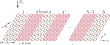
Let us start from the superlattice of strained silicene schematically shown in Fig. 1, where the number of the normal and strained regions with equal length L is N. The superlattice structure is indispensable for achieving the spin and valley filtering effect. In addition, the effect depends critically on the system parameters such as the local potential, the strain strength, and the Fermi energy. The electron current is evaluated along the x axis. The y axis is along the interface direction. For simplicity, a uniform strain is assumed along the y axis. The low-energy effective Hamiltonian of the strained silicene is given by
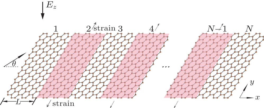 | Fig. 1. Schematic diagram of an alternative strained silicene. The strain is applied only to the pink region. An external electric field Ez is applied perpendicular to the whole silicene sheet and triggers a staggered AB-sublattice potential Δ z. |

with Δ = η σ λ + Δ z. Here τ is the Pauli matrix in the sublattice pseudospin space; η , σ = ± 1 refer to two valleys of K and K′ in the Brillouin zone and spin indices (spin up and spin down), respectively; A is the effective gauge potential induced by the strain in the K and K′ valleys; λ denotes the SOC strength; and Δ z is the staggered sublattice potential between silicon atoms at A sites and B sites, which is adjustable by an external electric field Ez applied perpendicular to the silicene plane. In the normal region, A is set to zero (A = 0). From Hamiltonian (1), we can obtain the eigenvalues in the strained silicene,

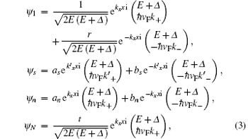
where k is the wave vector in the normal region. By defining the incident angle θ , we have kx = k cosθ and ky = k sinθ . Note that the wave vector is conserved in the y direction due to the translational invariance along the y axis. We define the first interface (from the left) between the normal and the strained regions as x = 0. Therefore, the wavefunction for valley η and spin σ in each region is
with 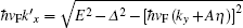
In order to obtain transmission coefficient t, we have to match the wavefunctions at the N − 1 interfaces. Then the relationship between reflection coefficient r and transmission coefficient t can be derived by the transfer matrix method, [9, 10]


The transmission probability of the electron that tunnels through the superlattice structure can be calculated as T = | t| 2.
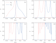
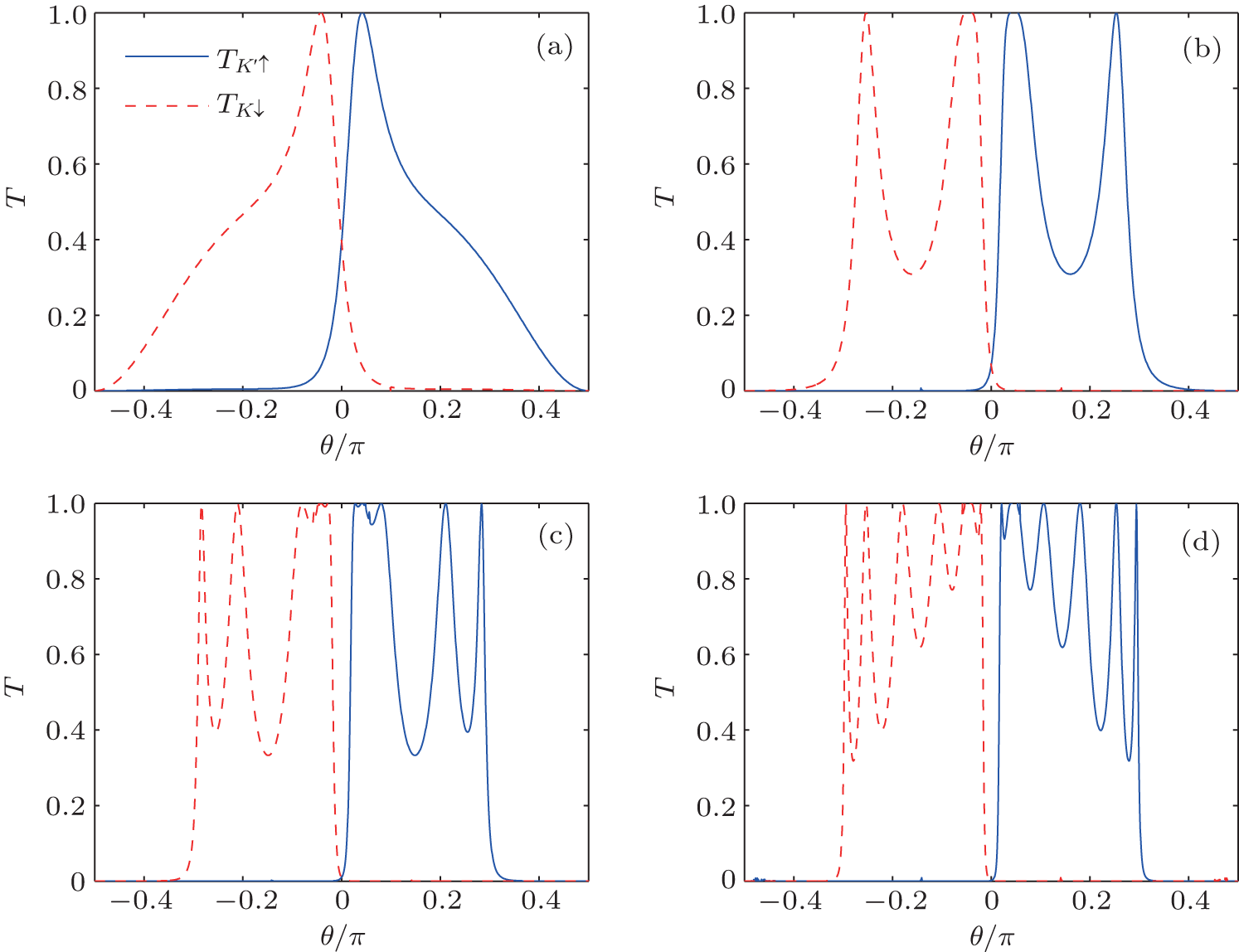
Based on the formulae above, we calculate the transmission of electrons T, which is very sensitive to the system parameters. We first consider the λ = Δ z = 0 case, since the valley splitting can be induced without the SOC and staggered sublattice potential. In the following, we set A = 1.9 meV, L = 2.1 nm, Fermi energy E = 2.1 meV, and Fermi wave vector kF = E/(ℏ vF) = 2.2 nm− 1. The transmission probability T as a function of incident angle θ for different N is plotted in Fig. 2. It shows that the valley-resolved transmission TK and TK′ are mirrored about θ = 0 (TK(ky) = TK′ (− ky)). This comes from the fulfilled time-reversal (TR) symmetry of the system. When N increases, T has a maximum value 2 for both valleys, but decreases rapidly for the K (K′ ) valley at θ > 0 (θ < 0), while it shows a more oscillatory pattern versus θ for the other valley. The range of θ that has mixed valley currents is also shrinking. The onset of vanishing mixed valley current occurs at N = 9, as confirmed in Fig. 2(d), where TK(K′ ) at θ > 0 (θ < 0) has been completely forbidden. So only one valley species is allowed to transmit at θ > 0 or θ < 0. This separation of the two valleys in the θ space (ky) renders the system an ideal angle-resolved valley filter.[15] The underlying reason for this intriguing result is that, during the tunneling, the small transmission probability of the mixed θ region decreases to zero when the superlattice number N increases.
 | Fig. 2. Valley-resolved transmission probability TK(K′ ) as a function of the incident angle θ for different numbers of alternating normal and strained regions in the system: (a) N = 3, (b) N = 5, (c) N = 7, and (d) N = 9. Parameters are A = 1.9 meV, L = 2.1 nm, E = 2.1 meV, and kF = E/ℏ vF) = 2.2 nm− 1. |
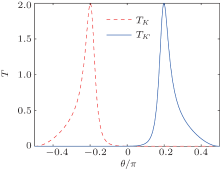
As a matter of fact, one can also achieve the same fully angle-resolved valley current by increasing the gauge potential A, even if the system does not have a superlattice structure. Figure 3 is plotted by taking the parameters N = 3 and A = 2.9, the other parameters remain the same as those in Fig. 2. In comparison with Fig. 2(a), an increase of A has the effect of blocking the transmission for K (K′ ) valley electrons at θ > 0 (θ < 0) like the increase of the superlattice number N, but it does not show as many oscillations as N > 3 does, which is ascribed to the resonant tunneling effect. From transverse momentum conservation and energy conservation at the interface
 | Fig. 3. Valley-resolved transmission probability TK(K′ ) as a function of the incident angle θ when the gauge potential A = 2.9 meV and the superlattice number N = 3. Other parameters are the same as those in Fig. 2. |
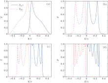
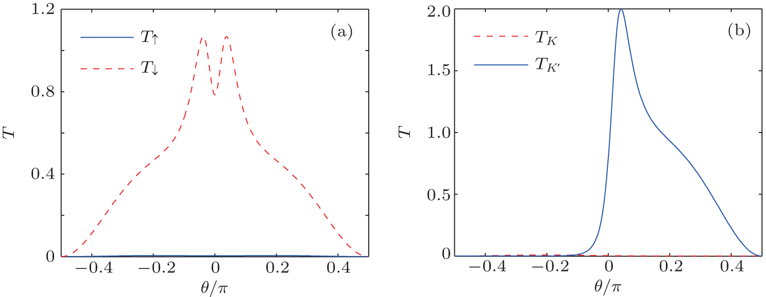
Now we are going to investigate the system with both SOC and staggered sublattice potential turned on. We set λ = Δ z = 1 meV and keep other parameters the same as those in Fig. 2. The numerical results of both spin- and valley-dependent transmissions are plotted in Fig. 4. It is seen that a similar pattern to that in Fig. 2 is obtained, but the maximum transmission probability is reduced to 1 because the valley-dependent transmission in Fig. 2 is attributed to two spin species. The curves of TK(K′ ) and T↓ (↑ ) are identical in this case. The reason is that in the presence of λ and Δ z, we can derive the energy gap 2| Δ | = 2| η σ λ + Δ z| from Eq. (2). Then it is straightforward to realize that the valley degree of freedom η and the spin degree of freedom σ are coupled together in the system, so the system has two states, namely, η σ = ± 1. However, the η σ = 1 state does not transmit through the system. Because in this state, EF≈ Δ , the wave vectors in the normal silicene region will be small (k ≈ kx ≈ ky ≈ 0) and 

 | Fig. 4. Valley and spin dependent transmission probability TK(K′ )/T↓ (↑ ) as a function of the incident angle θ . The superlattice numbers are taken as (a) N = 3, (b) N = 5, (c) N = 7, and (d) N = 9. Parameters are A = 1.9 meV, L = 2.1 nm, E = 2.1 meV, kF = E(ℏ vF) = 2.2 nm− 1, and λ = Δ z = 1 meV. |
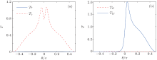
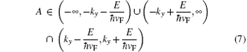
 | Fig. 5. (a) Spin-resolved transmission probability T↑ (↓ ) and (b) valley-dependent transmission probability TK(K′ ) versus the incident angle θ in the normal/strain/normal silicene system. A valley-dependent (a) or a spin-dependent (b) staggered potential is considered in calculations. Other parameters are the same as those in Fig. 4. |

if ky > 0 (ky < 0) and | A| is large enough and properly tuned, for the K (K′ ) valley, 


the interface will only permit filtering the K valley electrons; while
is for only filtering the K′ valley electrons.
From the above results, one can see that the total or angle-averaged transmission is still spin (T = T↑ + T↓ ) or valley (T = TK + TK′ ) degenerate since the system fulfills the time reversal symmetry. Thus, by introducing the factors breaking the time reversal symmetry, one can in principle obtain the whole spin or valley filtering effect. We first consider the valley-dependent staggered potential η Δ z, which comes from the circularly-polarized optical field to bring about the Floquet topological state or quantum anomalous Hall effect in honeycomb-lattice materials.[20] The term η σ λ + η Δ z replaces Δ in Hamiltonian (1). The transmission of each spin versus θ for N = 3 is plotted in Fig. 5(a) with the same parameters used in Fig. 4. Unsurprisingly, the transmission of spin-up electrons is entirely suppressed while that of the spin-down counterparts is still permitted regardless of θ . This is certainly very dependent on the parameters such as EF ≈ Δ . Therefore, the system performs as a spin filter effect.
How about a system whose electrodes have electrochemical potentials shifted by a staggered magnetization or spin-dependent staggered potential σ Δ z? Akin to the previous discussion, if we keep the parameters the same as those in Fig. 5(a), EF ≈ Δ satisfies for only the K valley, the system appears to be a perfect valley filter as shown in Fig. 5(b), since only the K′ valley electrons can transmit through the system.
Besides the spin or valley-dependent staggered potentials introduced in Hamiltonian (1) to achieve the spin or valley filtering effect, a simple factor breaking the time-reversal symmetry, such as a magnetic exchange field, is also feasible to fully filter spin or valley in our studied silicene system. By considering uniform magnetization in silicene from the magnetic proximity effect, as proposed for graphene, [21] the Hamiltonian for the strained region now reads

where h is the exchange field in the strained region. Notice that the time-reversal symmetry has been broken since we have introduced this ferromagnetic property. In the normal region, h = 0. We only consider the normal/strain/normal junction. Similar to the above, we obtain the eigenvalues of the Hamiltonian in the normal and strained silicene
and the transmission coefficient by matching the wavefunctions at the two interfaces

where EN = E + Δ , ES = EN + σ h, and u = ek′ xLi. Notice that when EN = ES, this expression becomes the one solved by Eq. (4) at N = 3. We can derive the transmission probability T subsequently.
We turn off the staggered sublattice potential Δ z in all the regions and plot the valley resolved transmission of this system versus the incident angle θ in Fig. 6. The parameters are the same as those in Fig. 2, except h = 1.1 meV. In this situation, the K valley electrons are almost blocked while the K′ valley electrons can still transmit through the junction. By further investigating this situation, a satisfactory valley filter can be obtained when | E| = | λ | + | h| . Obviously, due to the SOC, when we introduce a valley exchange field not the magnetic exchange one h, we could obtain the spin filter effect. Unfortunately, no such valley exchange field is found, and the valley-polarized metal can only stem from some combined effects such as the former-mentioned optical field plus the staggered potential.[20]
 | Fig. 6. Valley-resolved transmission probability TK(K′ ) as a function of incident angle θ of the normal/strain/normal silicene system. An exchange field is applied to the strained region. Parameters are the same as those in Fig. 2 and h = 1.1 meV. |
In summary, we have investigated the spin and valley transport in a strained silicene within a superlattice structure. It is shown that the opposite-valley gauged field from the strain can lead to a perfect angle-resolved spin or valley filtering effect when the intrinsic spin– orbit interaction is taken into account. When the spin- and valley-dependent staggered potentials are introduced into the system to break the time-reversal symmetry, there exists a perfect total spin or valley filtering effect and the system exhibits a spin or half-metal property. It is shown that a uniform magnetization in silicene through the magnetic proximity effect is also feasible to achieve the valley half-metal effect. Our findings might shed light on designing the spin- and valley-based electronic device by silicene.
| 1 |
|
| 2 |
|
| 3 |
|
| 4 |
|
| 5 |
|
| 6 |
|
| 7 |
|
| 8 |
|
| 9 |
|
| 10 |
|
| 11 |
|
| 12 |
|
| 13 |
|
| 14 |
|
| 15 |
|
| 16 |
|
| 17 |
|
| 18 |
|
| 19 |
|
| 20 |
|
| 21 |
|