Strain analysis of free-standing strained silicon-on-insulator nanomembrane*
[Sun Gao-Dia), b) , Dong Lin-Xia)†  , Xue Zhong-Ying
b) , Chen Dab) , Guo Qing-Leib) , Mu Zhi-Qiangb) ]
, Xue Zhong-Ying|
|


†Corresponding author. E-mail: donglinxi@hdu.edu.cn
*Project supported by the National Natural Science Foundation of China (Grant Nos. 61376117 and 61107025) and the Zhejiang Provincial Natural Science Foundation of China (Grant No. LY13F040004).
Based on the ultra-thin strained silicon-on-insulator (sSOI) technology, by creatively using a hydrofluoric acid (HF) vapor corrosion system to dry etch the SiO2 layer, a large area of suspended strained silicon (sSi) nanomembrane with uniform strain distribution is fabricated. The strain state in the implemented nanomembrane is comprehensively analyzed by using an UV-Raman spectrometer with different laser powers. The results show that the inherent strain is preserved while there are artificial Raman shifts induced by the heat effect, which is proportional to the laser power. The suspended sSOI nanomembrane will be an important material for future novel high-performance devices.
Strain engineering is widely applied to semiconductor materials to enhance their carrier mobility.[1, 2] Strained semiconductor nanostructures have been regarded as the fundamental building blocks for non-planar, multiple-gate, and thin-film transistor (TFT) architectures.[3] As a cost-effective and high-performance technique, applying strain in the fabrication of Si-based devices has gained significant attention since its first introduction.[4] In particular, by combining the merits of strained silicon (sSi) and silicon-on-insulator (SOI), namely strained silicon-on-insulator, devices with excellent performance can be realized. Furthermore, this technique is compatible with the standard silicon metal– oxide– semiconductor field-effect transistor (MOSFET) process, therefore a high integration level is guaranteed.[5]
Since the carrier mobility enhancement largely depends on the amount of strain in silicon that modifies its band structure, [6] investigating and understanding the strain behavior of sSi nanomembrane during various processing steps is a hot research topic. Nevertheless, most of the previous studies in the literature were focused on the average strain in the top sSi layer of the representative sSi/SiO2/Si structure. For instance, it was reported that the strain in the stained silicon layer could be retained during high temperature annealing.[7] Liu et al.[8] experimentally realized periodic arrays of strained silicon nano-stripes and nano-pillars on a thin relaxed-SiGe on insulator, and the influence of the size on the strain evolution was investigated. Utilizing the developed coherent X-ray diffraction (CXD) method, Xiong et al.[9] investigated the strain behavior in an individual ultra-thin sSOI structure with a high spatial resolution. Their results showed that the relaxation was localized near the structure edges, which undergo a significant contraction as a result of the patterning-induced free surfaces. Besides, it was reported that virtual strain can be recorded at different incident laser power densities when measuring the Raman spectra of suspended cluster nanowires.[10] Due to the local heat effect, the higher the excitation power, the more the total in-plane stress is determined. This is because when the laser power increases, and hence the temperature, the lattice will hydrostatically expand and the phonon frequency will redshift.[11] Moreover, other stdudies investigated the Raman artificial peak shift of suspended nanowires induced by the heat effect, where the air gaps might act as a micro cavity and increase the absorption caused by the Mie type scattering in the constriction parts.[12]
However, experimental studies of the strain evolution and the heat effect in the free-standing nanomembrane are still missing. This is mainly due to the adhesion existing in the traditional process with a wet chemical solution. When the SiO2 layer is etched away, a “ released” structure adhering to the substrate will be produced.[13] However, many high-performance strained Si-based devices, such as multi-gate, gate-all-around (GAA) nanowire MOSFETs and thin-film transistors, rely on the process of etching the buried SiO2 layer.[14] Thereafter, it is crucial to precisely detect the strain evolution and the heat effect in the strained suspended nanomembrane during the device fabrication process.
In this paper, based on the technology of the ultra-thin strained silicon-on-insulator, by creatively using the HF vapor corrosion system for dry etching the buried SiO2 to eliminate the adhesion, a large area free-standing sSi nanomembrane with uniform strain distribution is fabricated. The implemented free-standing sSi nanomembrane is characterized by optical microscopy, transmission electron microscopy (TEM), and scanning electron microscopy (SEM) respectively. The virtual strain induced by the heat effect in both suspended Si and sSi nanomembranes is comprehensively analyzed by using an UV-Raman spectrometer with different laser power.
This study investigates the strain evolution and the heat effect in the strained free-standing nanomembrane. The results show that the inherent strain is preserved, while there are artificial Raman shifts due to the heat effect, which is proportional to the excitation power in the suspended nanomembrane.
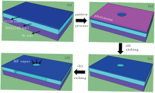
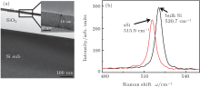
The 8-inch sSOI wafers were used in this particular study. The biaxial strain was generated by the hetero epitaxial growth of Si thin layers on a relaxed Si0.75Ge0.25 layer. As previously reported, a layer transfer method involving direct wafer bonding, hydrogen ion-induced thin layer transfer, and etch-back methodology was adopted to fabricate the tensile strained layer.[15] After patterning by electron-beam lithography (EBL) and reactive ion etching (RIE), the buried SiO2 layer of the specimen was dry etched to release the structure via an HF vapor corrosion system. The system parameters were HF gas flow rate 400 sccm, alcohol 410 sccm, and temperature 60 ° C. The schematic diagrams of the pattern processing and the dry etching are shown in Fig. 1. The cross-sectional transmission electron microscopy image of the sSOI sample is shown in Fig. 2(a). The measured thickness of the top layer is 18 nm, as shown in the inset of Fig. 2(a).
 | Fig. 1. Schematic diagrams of pattern processing and dry etching. |
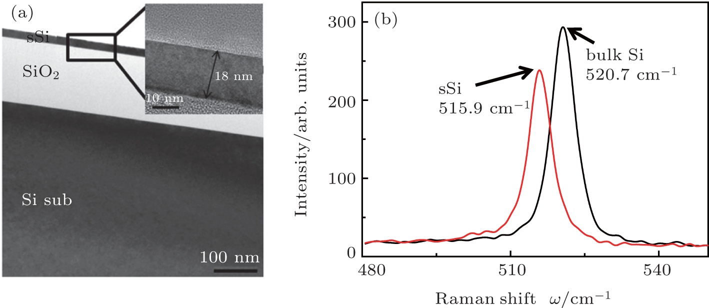 | Fig. 2. (a) Cross-sectional TEM image of sSOI sample, (b) Raman spectra of strained silicon and bulk Si. |
The strain state in the sSi nanomembrane was characterized at room temperature by using a confocal UV-Raman scattering spectrometer (JY LabRam HR800) equipped with an UV He– Cd 325 nm laser and a 2400 line/mm grating. A 40× objective was used to focus the incident laser beam to a spot size of 1 μ m on the sample surface. The incident applied laser power was attenuated to one-tenth of the initial power. It is worth noting that the penetration depth of the UV laser (325 nm He– Cd laser) in Si is approximately 8 nm, so the obtained Raman signal only comes from the top strained Si nanomembrane within 8 nm thickness; any interference from the substrate is removed.[16] The strain in the bulk Si and the sSi layer was detected by the UV micro-Raman spectrometer, which can be calculated from the empirical formula[17, 18]

where ω bulk and ω strained denote the peak positions (cm− 1) for the bulk Si and the strained Si, respectively; 0.123 is the inverse strain-phonon coefficient (cm); and ε is the biaxial strain (%). The typical Raman spectrum of the sSOI features a peak at 515.9 cm− 1, corresponding to 0.59% initial biaxial tensile strain in the original sSOI, as displayed in Fig. 2(b).
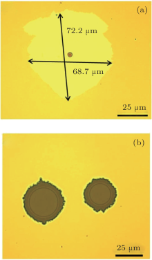
Figure 3(a) shows the optical microscope picture of the time-controllable suspended sSi nanomembrane. Obviously, there is a clear corrosion boundary circle line after HF etching the buried SiO2 layer through the pre-open hole. The black circle hole represents the top sSi etched by EBL and RIE. The HF etching results in the irregular boundary line shape. The size of the suspended nanomembrane is about 72.2 μ m × 68.7 μ m, and the buried SiO2 layer is fully etched away due to its small thickness of 145 nm. The size of the suspended nanomembrane is extremely large when compared with what can be produced with the wet etching method, which is usually around hundreds of square microns. The optical microscope picture in Fig. 3(b) displays an sSi nanomembrane sticking to the substrate (not suspended). This verifies that the previous sSi nanomembrane is free-standing.
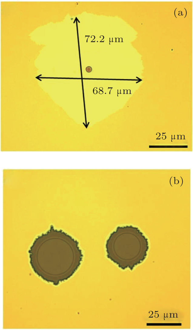 | Fig. 3. Optical microscope pictures of (a) the suspended sSi nanomembrane and (b) the sSi nanomembrane sticking to the substrate. |
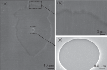
In order to gain deeper insight into the suspended strained Si nanomembrane, we obtain the surface topography of the top strained layer by using a scanning electron microscope. Figure 4 displays the SEM images of the whole and the local suspended structures. In Fig. 4(a), we can see the same contour structure in Fig. 3(a). Furthermore, we find the rough buried SiO2 layer in Fig. 4(b) by zooming in the edge of the suspended structure. It is verified that the top strained layer is detached from the buried SiO2 layer, as shown in Fig. 4(c).
 | Fig. 4. SEM images of (a) the whole and (b)– (c) local regions of the suspended sSi nanomembrane. |
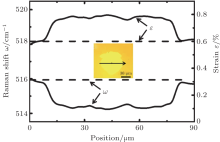
Figure 5 shows the evolution of the strained Si– Si Raman peak position and the corresponding in-plane strain obtained from Eq. (1) along the Raman line scan across the suspended structure shown in the inset. The dashed lines show the origin strain and the corresponding Raman peak position of the sSOI sample for comparison. It is clearly observed that the lowest Raman peak coming from the suspended region of the patterned structure locates at 514.2 cm− 1, which is ∼ 1.7 cm− 1 downshift from the initial value. The Raman peak positions of the suspended regions have a tiny fluctuation around 514.2 cm− 1, indicating that the strain is uniformly distributed. This downshift of the Si– Si peak position indicates an increase in the biaxial tensile strain from 0.59% to 0.8%. It is worth noting that the interferential spectra measured from the circle hole of the substrate have been removed.
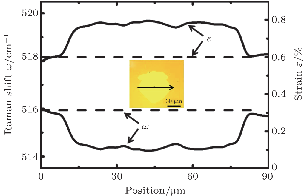 | Fig. 5. Strain distribution and Raman shift of the suspended sSi nanomembrane along the Raman line scan shown in the inset. |
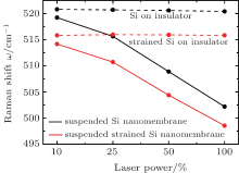
The Raman peak positions of SOI and sSOI suspended nanomembranes with different laser powers are shown in Fig. 6. The Raman peaks of the sSOI nanomembrane without HF etching exhibits a small variation (located at about 515.9 cm− 1) with different laser power. On the contrary, the peak of the suspended sSi nanomembrane with HF etching dramatically shifts to the lower wavenumber as the laser power increases, indicating that the nanomembrane becomes highly strained. It is interesting to note that the conventional SOI wafer without strain exhibits a similar behavior with the sSOI. This tells us that the power-dependent heat effect also exists in the SOI. In other words, when the buried SiO2 layer is etched away, the free-standing nanomembrane is very sensitive to the power of the excitation laser for both strained Si and unstrained Si. While, due to the high absorption of the substrate, the peak positions of both unsuspended strained Si and unstrained Si have tiny shifts from the origin, even excited at high power. We have[19]
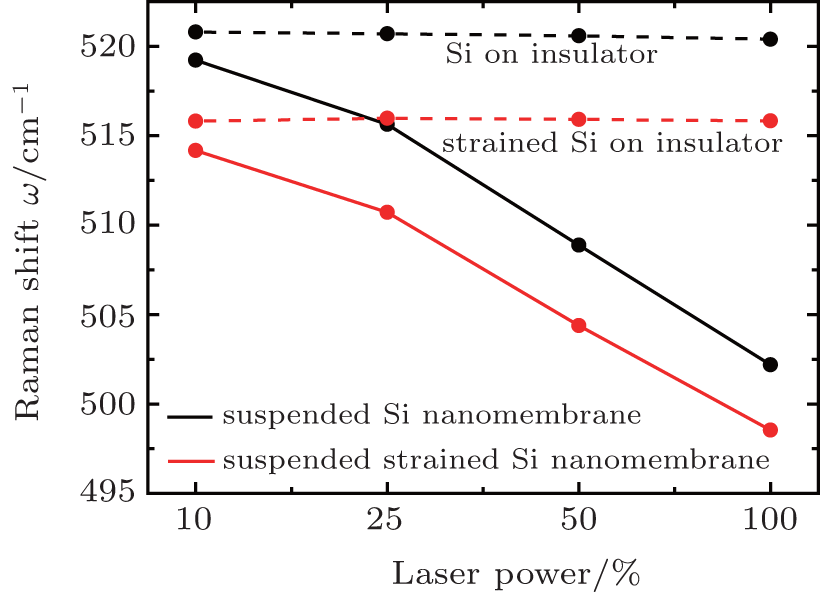 | Fig. 6. Raman spectra of SOI and sSOI suspended nanomembranes with different incident excitation laser powers. The laser power is given by the percentage to the initial power. Dashed lines denote the Raman spectra of SOI and sSOI samples without any treating for comparison. |

where q is the inside heat flux, P is the continuous-wave incident laser power, w is the full width at half-maximum, and x and y denote the laser measuring lateral directions. The heat absorption coefficients of the etched region are α suspended layer = 1.5% and α substrate = 2.7%, whereas α unsuspended layer = 0.8% and α substrate = 12.3% for regions of the untreated sample. The increased absorption of the suspended nanomembrane may be caused by the phonon– boundary scattering, which leads to a reduction of the thermal conductivity.[20] According to the thermal conductivity theory based on the solution of the Boltzmann transport equation, the reduced phonon mean-free paths further explain the variation of the phonon transport in the ultrathin sSi films.[21] It has also been reported that the phonon transport in the nanomembrane could be drastically modified by (i) changes in the phonon disperison relation; [22] and (ii) enhanced boundary scattering. The phonon group velocities in the nanomembrane would be considerably smaller than the bulk value, which is altered by the phonon dispersion relation. On the other hand, measuring the Raman shift of the suspended nanostructure at ambient pressure gives rise to the convection, which influences the temperature distribution.[12] According to the above discussion, etching away the buried SiO2 layer results in a significant change in the absorption of the top nanomembrane. Comparing the Raman spectra of SOI and sSOI obtained with the same power, we can see nearly the same deviation (1.7 cm− 1 downshift) for the suspended peak positions from the unsuspended ones. This discrepancy belongs to the “ virtual strain” caused by the heat effect on the suspended nanostructure, and the inherent strain is preserved.
We fabricate a large free-standing sSi nanomembrane by dry etching the SiO2 layer. A comprehensive analysis shows that virtual strain exists in both suspended Si and sSi nanomembranes. Besides, the strain behavior of the suspended nanomembrane indicates that the free-standing nanomembrane is very sensitive to the laser power. Therefore, it must be taken into account in practice when designing nano-devices based on the sSi suspended nanomembrane.
| 1 |
|
| 2 |
|
| 3 |
|
| 4 |
|
| 5 |
|
| 6 |
|
| 7 |
|
| 8 |
|
| 9 |
|
| 10 |
|
| 11 |
|
| 12 |
|
| 13 |
|
| 14 |
|
| 15 |
|
| 16 |
|
| 17 |
|
| 18 |
|
| 19 |
|
| 20 |
|
| 21 |
|
| 22 |
|