
Preparation of SiO2@ Au nanorod array as novel surface enhanced Raman substrate for trace pollutants detection*
[Hou Meng-Jinga) , Zhang Xiana) , Cui Xiao-Yanga) , Liu Cana) , Li Zheng-Caob) , Zhang Zheng-Junb)†  ]
]
]
|
|


†Corresponding author. E-mail: zjzhang@tsinghua.edu.cn
*Project supported by the National Basic Research Program of China (Grant No. 2013CB934301), the National Natural Science Foundation of China (Grant No. 50931002), the Research Project of Chinese Ministry of Education (Grant No. 113007A), and the Initiative Scientific Research Program of Tsinghua University, China
An effective surface enhanced Raman scattering (SERS) substrate is designed and fabricated by synthesis of SiO2 nanorods array via glancing angle deposition, followed by coating Au nanoparticles onto SiO2 surface in order to create numerous “hot spots”. The detecting sensitivity of such substrate could be optimized by simply adjusting the deposition time of Au. Thus, it can be used for detection of Rhodamine 6G at concentration as low as 10−9 M. Furthermore, our SERS substrate is applied to detect 5 μg/g polychlorinated biphenyls in soil sample, which proves its potential for trace environmental pollutants detection.
Considering the necessity to discover the harmful substances in the environment from which human health suffers, accurate and convenient ways are called for to realize pollutants detection.[1– 4] Among the detecting methods, the ones based on the surface enhanced Raman scattering (SERS) effect have drawn a great deal of attention for they can show the characteristic chemical construction of molecules despite the low concentration.[5– 9] It has been confirmed that Ag and Au are the best SERS active materials, which could improve the Raman scattering signal obviously, [10] while Au is certainly more stable. In recent years, SERS substrates such as Ag or Au nanorods, nanowires, and mesoparticles were fabricated and they performed good detecting ability.[11– 15] However, noble metals were consumed, and most of the fabrication processes were complicated. Therefore, many hybrid systems of Au and oxides were studied in previous works. Tian et al. coated Au nanoparticles with silica shell so that the multipolar interaction between the Au @SiO2 nanoparticles and gold film contributed greatly to the SERS.[16] Some researchers attached Au or Ag onto oxides to obtain obvious SERS effect.[17– 19] In this work, a Au nanoparticles decorated SiO2 nanorods array was fabricated as the SERS substrate with the method of physical vapour deposition (PVD) completely. Compared to other three-dimensional SERS substrates fabricated with chemical methods, [15, 20, 21] it possesses advantages of high purity and repeatability of the fabrication process. Therefore, the SERS substrate is very sensitive when detecting environmental pollutants.
According to the theory of electromagnetic enhancement mechanism, Au nanoparticles and the gaps between them act as “ hot spots” which could generate a strong electromagnetic field and improve the Raman signal intensity of the probe molecules adsorbed on them.[22, 23] Meanwhile, the SiO2 nanorods are transparent to visible light, [24] which enables more incident light as well as scattering light reach the “ hot spots” . The trace detecting ability of this kind of SERS substrate was tested by Rhodamine 6G (R6G) solution. Samples with different amount of Au nanoparticles were immersed by 10− 6 M R6G solution, resulted in Raman peaks intensity obviously relating to Au depositing time. Among the series samples, the best one could detect 10− 9 M R6G, which confirmed the SERS substrate was quite effective.
The optimized SERS substrate was then employed to detect trace polychlorinated biphenyls (PCBs) extracted from soil sample. As a series of toxic chemicals, PCBs are widespread in the environment and may accumulate in human body, even causing cancer.[25] Hence, it is necessary to detect trace PCBs in realistic samples. The characteristic Raman peaks of PCBs were clearly shown in the spectrum obtained from the extract solution, which demonstrates the substrate is useful in environment pollutants detection.
The SiO2 nanorods were deposited on Si (100) substrates in a DZS-500 electron beam evaporation system (SKY Technology Development Co., Ltd. Chinese Academy of Sciences) with a background vacuum level of 10− 4 Pa, by the glancing angle deposition (GLAD) technique. During deposition, the substrate was rotated at a speed of 2 rpm, and the incident angle of the SiO2 beam was fixed at 86° , with a depositing rate of ∼ 5 Å /s measured by a quartz crystal microbalance. After deposition, Au nanoparticles were deposited on the SiO2 nanorods with a SBC-12 vacuum ion coater (KYKY Technology Co., Ltd.). The coating time was controlled from 30 seconds to 180 seconds, respectively. The morphology and structure of these samples were characterized with a JSM-7001F scanning electron microscope (SEM) and a JEM-2011 transmission electron microscope (TEM), respectively.
The performances of these SiO2@Au nanorods samples as SERS substrates were evaluated by a HR800 micro-Raman spectrometer (HORIBA JOBIN YVON), using a 633-nm He– Ne laser as the excitation source, and Rhodamine 6G (R6G) as the probe molecule. The R6G powder was dissolved in deionized water and was diluted to concentrations from 10− 5 M to 10− 9 M. The SERS substrates were immersed into the R6G solutions for 30 minutes, and then dried naturally in air. During the Raman scattering measurement, the diameter of the laser beam was fixed at ∼ 1.2 μ m, and the integration time of each spectrum was fixed at 30 seconds.
To check the possibility of using these structures as SERS substrates to detect PCB pollutants in our environment, we used the real PCB-polluted soil provided by the Institute of Soil Science, Chinese Academy of Sciences as an example. 0.2 g PCBs-polluted soil whose concentration of PCB is 5 μ g/g was mixed with 20 mL acetone, stirred with magnetic stirring apparatus for 30 minutes, and left to stand for 1 hour. After the soil precipitated, the clear supernatant liquid with a concentration of ∼ 10− 7 M was transferred by a pipette into another beaker. The SERS substrate was immersed into the liquid for 1 hour to adsorb PCB molecules, and then dried naturally. Afterwards, the Raman spectrum of the PCBs was measured, and the integration time was fixed at 60 seconds.
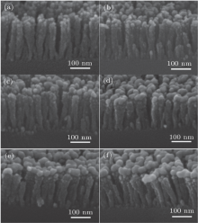
Through the method of electron beam deposition, a SiO2 nanorod array was fabricated. The SiO2 nanorods are about 170 nm in length, and their diameters are around 30 nm. We could see from the SEM photos (Fig. 1) that the nanorods were fabricated with appropriate spacing and tough surface, while decorated by Au nanoparticles deposited by sputtering a Au target for different times. Along with the increase of the Au depositing time, the amount of Au nanoparticles increases. There are few particles on the rods at the initial stage of the depositing process, and then more particles aggregate on the upper parts of the nanorods when the Au depositing time reaches 150 s or longer, while the nanorods are still separated from each other.
 | Fig. 1. SEM morphology of SiO2@Au nanorods array. Depositing times of Au nanoparticles are (a) 30 s, (b) 60 s, (c) 90 s, (d) 120 s, (e) 150 s, and (f) 180 s, respectively. |
Figures 2(a) and 2(b) show TEM images of the SiO2 nanorods decorated with Au nanoparticles of 120 seconds sputtering. The whole SiO2 nanorods were decorated homogeneously by Au nanoparticles whose diameter ranged from 3 nm to 10 nm. At the top of the nanorods, the nanoparticles are crowded, while the ones at the sidewalls were sparsely dispersed.
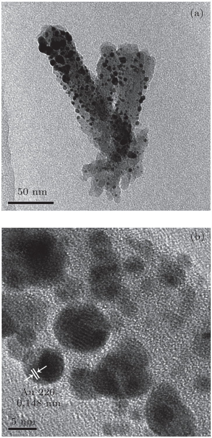 | Fig. 2. (a) TEM morphology of SiO2@Au nanorods. (b) HRTEM of a region on the SiO2@ Au nanorod, and the dark parts are Au nanoparticles. |
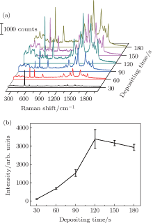
The performance of these samples as a SERS substrate was examined utilizing 10− 6 M R6G as the analyte. Figure 3(a) shows the Raman spectra of the R6G molecules adsorbed on the samples with different amounts of Au nanoparticles. We find that the intensity of the Raman spectrum is highly dependent on the Au depositing time. To make a clear comparison, the intensity of the Raman peak at ∼ 612 cm− 1 of R6G is plotted in Fig. 3(b) versus the depositing time of Au nanoparticles. For each sample, eight points are selected randomly and measured. The intensity in the figure is the average value of these data, and the error bars are also shown. The deviations are kept at less than 20% for all of the samples, which shows the good reproducibility of the PVD fabricating SERS substrate. The Raman intensity first increases with increasing depositing time of Au, and when the depositing time surpasses 120 s, the Raman intensity decreases. The reason for this phenomenon could be that, when the depositing time is less than 120 s, more nanoparticles were deposited on SiO2 nanorods, hence inducing an increase in the intensity of the Raman signals, due to the generation of more “ hot spots” and possible coupling enhancement caused by the decrease in the distance of neighboring nanoparticles.[24, 26– 28] Meanwhile, with the increase in the number of nanoparticles, more nanoparticles gathered on the top of the nanorods (see Figs. 2(a) and 2(b)), thus leading to coalescence of the Au nanoparticles, which in return weakens the enhancement of the Raman signals. These measurements suggest that 120 s is an optimal depositing time of Au nanoparticles on SiO2 nanorods to form the SERS substrate.
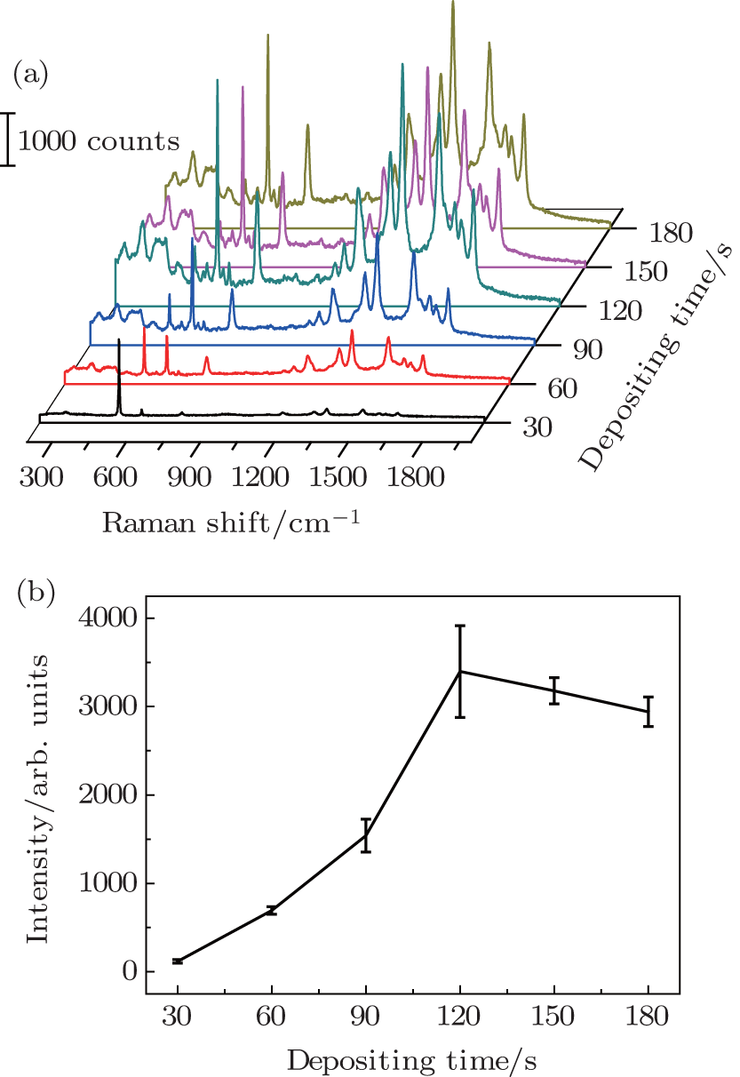 | Fig. 3. (a) Raman spectras of 10− 6 M R6G adsorbed on the SERS substrates whose Au depositing times are 30 s, 60 s, 90 s, 120 s, 150 s, and 180 s respectively. (b) Intensity of 612 cm− 1 peak in the Raman spectrums in Fig. (a). |
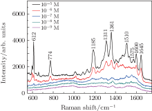
The SiO2 nanorods coated with Au nanoparticles by 120 s deposition is further examined by measuring its SERS sensitivity with R6G molecule using differently concentrated solutions, i.e., from 10− 5 to 10− 9 M. From the obtained Raman spectra in Fig. 4, the characteristic peaks of the R6G molecule are clearly shown, i.e., the 612 cm− 1 peak stands for C– C– C ring in-plane vibration, 774 cm− 1 peak stands for C– H out-of-plane bend, 1185 cm− 1 peak refers to C– C stretching vibrations, the 1311 cm− 1 and 1575 cm− 1 peaks stand for N– H in-plane bend, while the 1361 cm− 1, 1510 cm− 1, and 1645 cm− 1 peaks stand for C– C stretching.[29– 32] For solutions of lower concentrations, despite the fact that the intensity of the Raman signals is reduced, the characteristic peaks could still be observed. Therefore, the detection limit of R6G molecules using this SERS substrate should be around 10− 9 M. The SERS enhancement factor (EF) is also calculated by[20]
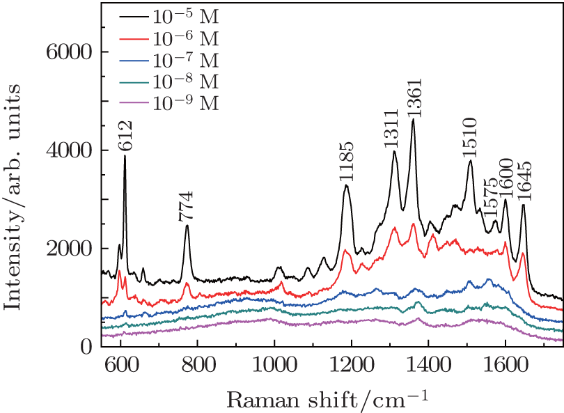 | Fig. 4. Raman spectrums of 10− 5 M, 10− 6 M, 10− 7 M, 10− 8 M, and 10− 9 M R6G adsorbed on SERS substrates whose Au depositing time is 120 s. |

where ISERS and Iref refer to the Raman intensity of R6G measured on the SERS substrate and independently, respectively, while the cref and cSERS refer to the concentrations of R6G molecules. As a result, the EF is about 106, which is extremely high for Au SERS substrate.
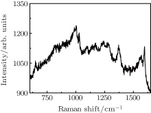
This kind of SERS substrate could be applied to detect pollutants dispersed in the environment. In this study, a soil sample which contains PCBs is chosen to test the detecting ability of the novel SERS substrate. Figure 5 is the Raman spectrum of the adsorbed PCBs which are extracted from the soil. Several peaks are relatively strong compared to the noisy peaks. The peaks near 1000 cm− 1 are attributed to the benzene ring breathing vibration, the region between 1590 cm− 1 and 1600 cm− 1 refers to benzene stretching vibration, and the peak at about 1030 cm− 1 stands for C– H in-plane deforming, so it could be determined that there is a benzene ring in the pollutant. Moreover, the peaks near 1280 cm− 1 stand for a biphenyl C– C bridge stretching vibration. Foremost, the peaks at about 650 cm− 1, 1170 cm− 1, and 1240 cm− 1 are assigned to C– Cl stretching vibration.[8, 9, 33– 35] Thus, it indicates that about 5 μ g/g PCBs existing in a soil sample could be detected successfully. This excellent performance proves that the optimized SERS substrate has potential applications in environmental pollutants detection.
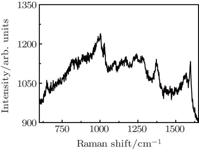 | Fig. 5. Raman spectrum of PCBs which is extracted from soil sample adsorbed on the SERS substrate whose Au depositing time is 120 s. |
In this study, a kind of facile fabricated and economic SERS substrate is designed and optimized. The substrate possesses abundant “ hot spots” which are formed by Au nanoparticles adhered on the SiO2 nanorods, and could reach the detection limit of 10− 9 M R6G. Moreover, the substrate is applied to detect trace PCBs existing in soil sample and shows potentiality in trace environment pollutants detection.
| 1 |
|
| 2 |
|
| 3 |
|
| 4 |
|
| 5 |
|
| 6 |
|
| 7 |
|
| 8 |
|
| 9 |
|
| 10 |
|
| 11 |
|
| 12 |
|
| 13 |
|
| 14 |
|
| 15 |
|
| 16 |
|
| 17 |
|
| 18 |
|
| 19 |
|
| 20 |
|
| 21 |
|
| 22 |
|
| 23 |
|
| 24 |
|
| 25 |
|
| 26 |
|
| 27 |
|
| 28 |
|
| 29 |
|
| 30 |
|
| 31 |
|
| 32 |
|
| 33 |
|
| 34 |
|
| 35 |
|