Zhang Jun, Guo Yu-Feng†, Xu Yue, Lin Hong, Yang Hui, Hong Yang, Yao Jia-Fei. One-dimensional breakdown voltage model of SOI RESURF lateral power device based on lateral linearly graded approximation* . Chinese Physics B, 2015, 24(2): 028502
Permissions
One-dimensional breakdown voltage model of SOI RESURF lateral power device based on lateral linearly graded approximation*
Zhang Jun, Guo Yu-Feng†, Xu Yue, Lin Hong, Yang Hui, Hong Yang, Yao Jia-Fei
College of Electronic Science and Engineering, Nanjing University of Posts and Telecommunications, Nanjing 210003, China
Project supported by the National Natural Science Foundation of China (Grant No. 61076073) and the Specialized Research Fund for the Doctoral Program of Higher Education of China (Grant No. 20133223110003).
Abstract
A novel one-dimensional (1D) analytical model is proposed for quantifying the breakdown voltage of a reduced surface field (RESURF) lateral power device fabricated on silicon on an insulator (SOI) substrate. We assume that the charges in the depletion region contribute to the lateral PN junctions along the diagonal of the area shared by the lateral and vertical depletion regions. Based on the assumption, the lateral PN junction behaves as a linearly graded junction, thus resulting in a reduced surface electric field and high breakdown voltage. Using the proposed model, the breakdown voltage as a function of device parameters is investigated and compared with the numerical simulation by the TCAD tools. The analytical results are shown to be in fair agreement with the numerical results. Finally, a new RESURF criterion is derived which offers a useful scheme to optimize the structure parameters. This simple 1D model provides a clear physical insight into the RESURF effect and a new explanation on the improvement in breakdown voltage in an SOI RESURF device.
Keyword:
85.30.De; 85.30.Tv; 84.70.+p; SOI; RESURF; breakdown voltage; 1D model
Reduced surface field (RESURF) technology has been widely used in the high voltage integrated circuit (HVIC) and the smart power integrated circuit (SPIC) to improve the trade-off between specific on-resistance and breakdown voltage in the high-voltage transistor.[1– 7] Silicon on insulator (SOI) technology avoids the adverse effect of substrate on the device via inserting a buried oxide (BOX) layer between the substrate and the SOI layer. Due to the electrical isolation by BOX, SOI RESURF has the advantages of low leakage current, higher switching speed, considerable reduction in parasitic capacitance, and so on compared with the bulk silicon RESURF device.[6– 14] Meanwhile, the breakdown mechanism of SOI RESURF is different from that of bulk silicon RESURF.[13– 16] The study on the breakdown model is helpful to ascertaining the breakdown mechanism and providing guidance on structural optimization design. In the past two decades, researchers have proposed a variety of SOI RESURF models, which in general can be divided into two categories: a one-dimensional (1D) model and a two-dimensional (2D) model. The 1D model analyzes the 2D problem by decomposing it into two separate 1D problems at vertical and lateral directions respectively. Meanwhile, the 2D model gives a 2D electric field distribution and a 2D breakdown voltage by directly solving the 2D Poisson equation within the drift region. Due to the decoupling of 2D effects in the drift region, the 1D model is simple but fails to accurately describe the field potential distribution within the device.[5, 9, 10] Although 2D models can effectively analyze the 2D electric field and potential distribution, mathematical expressions are very complicated and lacking in clear physical meaning.[7– 12]
In this paper, we present a simple 1D analytical RESURF model of the SOI lateral power device based on charge sharing and lateral graded approximation. It is suggested that a lateral junction with linearly effective doping concentration should consider the 2D coupling effect and give a novel explanation for the lateral field reshaping/reduction effects. The breakdown voltages are investigated for both the incompletely and completely depleted drift region. Further, a new RESURF criterion is derived which can provide the accurate and reasonable estimation of the limitation of the device parameters. The calculated results are in good agreement with simulations, verifying the correctness of the model.
2. Analytical model
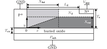
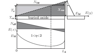
The schematic cross section of the SOI lateral RESURF structure is illustrated in Fig. 1. The electrical connection between the substrate and the active layer is blocked by a buried oxide layer (the thickness referred to as Tox), and the depletion region terminates on the surface of the buried oxide layer. A coordinate system is shown in Fig. 1. At a given applied voltage Vapp, the lateral P+ Nd junction is reverse biased. The lateral and vertical depletion widths of the drift region are Xlat and Xver, respectively. The overlap between the lateral and vertical depletion regions occurs, and a charge-sharing region is formed. We propose that charges in the sharing region are divided into two parts along the diagonal: the upper part contributes to the P+ Nd junction while the lower part contributes to the vertical structure. Hence, the single side abrupt P+ Nd junction is translated into a single side linearly graded P+ Neff(x) junction. As a result of charge coupling in the shared depletion region, the equivalent doping concentration of the lateral structure (Neff) can be expressed as a linear function:
where Ld is the length of the drift region, Nd is the doping concentration of the drift region, and Ts is the thickness of the SOI layer. η = Xver(Vapp)/Ts is the ratio of the vertical depletion region width to the SOI layer thickness, which indicates the coupling degree between lateral and vertical structures. The potential function ϕ (x) in silicon film is governed by the Poisson equation:
where q is the electronic charge, E(x) is the surface electric field, and ɛ s is the dielectric constant of silicon.
According to the breakdown condition, the following discussion is divided into four cases.
Fig. 1. Drift region charge-sharing effect in SOI RESURF device.
2.1. Partial-depletion breakdown
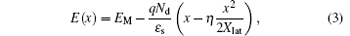
When the drift region is highly doped, the lateral breakdown occurs at the P+ Nd junction with the drift region partially depleted. As shown in Fig. 2, the surface electric field presents a peak at the P+ Nd junction and continuously drops to zero until the depletion region boundary. In this case, Xlat< Ld, Xver< Ts, and η < 1. Substituting Eq. (1) into Eq. (2) leads to the surface electric field distribution as follows:
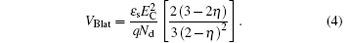
where EM is the maximum electric field. The breakdown occurs when EM approaches to the critical electric field of silicon EC. By substituting the boundary conditions E(0) = EC and E(Xlat) = 0 into Eqs. (2) and (3), the lateral breakdown voltage VBlat is expressed as
When η = 1, the drift region is just fully depleted, and the breakdown voltage follows VBlat = 1.17VBpn, where VBpn = ɛ sE2C/(2qNd) is the breakdown voltage of a conventional 1D planar diode.[3] Therefore, when η = 1, the RESURF structure enables the increase in the breakdown voltage by as much as 16.67% in comparison with that of the conventional 1D planar diode.
Moreover, from the vertical electric field distribution as shown in Fig. 2, a generalized single expression for the vertical partial-depletion breakdown voltage can be obtained as
where K = ɛ s/ɛ ox ≈ 3 is the dielectric constant ratio between silicon material and silicon dioxide material. However, when under the partial-depletion condition, owing to the severe degradation of the lateral breakdown voltage, the breakdown voltage is determined by the lateral P+ Nd junction.[3, 4]
Fig. 2. Schematic diagram of the charge-sharing region, the lateral equivalent doping concentration and the electric field distribution when 0 < η < 1
2.2. Lateral breakdown at P+ Nd junction for full-depletion case
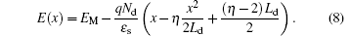
If the drift region is doped lowly enough, the charge-sharing effect between the vertical and lateral structure become more obvious, which results in the fact that the drift region is fully depleted (Xver ≥ Ts and η ≥ 1). Owing to the block of highly doped N+ region, the lateral depletion width is equal to the length of the drift region (Xlat = Ld). When η ≥ 1, as equation (1) shows, Neff(Ld) ≤ 0. The N-type drift region near the NdN+ junction behaves as an equivalent P-type doping region. Such a reversed equivalent PdN+ junction leads to a new electric field peak as shown in Fig. 3. This is because the charge density in the shared region that contributes to the vertical structure exceeds the doping concentration. Substituting Eq. (1) into Eq. (2) leads to the surface electric field distribution as follows:
Since the electric field peak at the P+ Nd junction is still higher than that at the NdN+ junction (E(0) > E(Ld)), the lateral breakdown occurs at the P+ Nd junction. As figure 3 shows, the equivalent doping concentration satisfies ❘ Neff(Ld)❘ < Nd, namely 1≤ η < 2. The lateral breakdown voltage VBlat can be given by substituting boundary condition E(0) = EC into Eqs. (2) and (6) as follows:
Under the full-depletion conditions, the lateral structure is composed of three PN junctions: P+ Nd, NdPd, and the equivalent PdN+ junction. The P+ Nd and equivalent PdN+ junction are reverse biased while the NdPd junction is forward biased. Therefore, both sides of the drift region have an electric field peak while a field valley appears at the middle of the drift region. This phenomenon fails to be explained by the other 1D model.[3, 5, 9, 10]
Fig. 3. Schematic diagram of the charge-sharing region, the lateral equivalent doping concentration and the electric field distribution when 1 < η < 2.
2.3. Lateral breakdown at NdN+ junction for full-depletion case
If the SOI layer is doped very lowly, the drift region is fully depleted before lateral breakdown occurs, and the highest surface electric field peak appears at the NdN+ junction (E(Ld) = EM). In such a case, as figure 4 shows, Neff(Ld) > Nd and η ≥ 2. By substituting Eq. (1) into Eq. (2), the surface electric field distribution is obtained as follows:
The lateral breakdown voltage VBlat can be derived by substituting boundary condition E(Ld) = EC into Eq. (2) and Eq. (8):
Especially, when η = 2, the equivalent doping concentration at the midpoint of the drift region is zero. The surface electric field distribution is completely symmetrical along the midline of the drift region, and the peak electric fields at both ends of the drift region are equal to the critical electric field of silicon (EC). In this case, P+ Nd and NdN+ junctions breakdown simultaneously, and the lateral breakdown voltage is maximized.
Fig. 4. Schematic diagram of the charge-sharing region, the lateral equivalent doping concentration and the electric field distribution when η > 2.
2.4. Vertical breakdown for full-depletion case
Owing to the existence of an oxide layer, the electrical connection between the substrate and the active layer is blocked, and the vertical depletion region ends at the Si– SiO2 interface.[1, 2, 14] Typically, the drift region is already fully depleted (Xver > Ts) when vertical breakdown occurs.[3, 4, 5] Figures 3 and 4 illustrate the profile of the vertical electric field. Accordingly, the vertical full-depletion breakdown voltage follows:
Note that in deriving Eqs. (5) and (10), it is assumed that Ts is much larger than the depth of the diffusion region xjn. If xjn is considered, Ts should be replaced by (Ts– xjn). It is evident that the breakdown voltage of the complete SOI RESURF is the minimum value between lateral and vertical breakdown voltages. In other words
3. Results and discussion
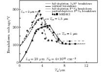
To demonstrate the viability and simplicity of the solution method, the results from analytical expressions are compared with numerical simulations by MEDICI, a commercial TCAD tool. Figure 5 demonstrates the modeled and simulated breakdown voltages each as a function of the thickness of the SOI layer. The calculated results are in good accordance with the simulations except for a few small discrepancies. As figure 5 shows, with the increase of Ts, the breakdown goes through four stages for the thinner buried oxide layer. 1) When Ts is very thin, the drift region is fully depleted and the breakdown occurs at the NdN+ junction (η ≥ 2). Accordingly, two electric field peaks appear at the NdN+ and P+ Nd junctions, and the overall breakdown voltage is determined by Eq. (9). 2) With the increase of Ts, the lateral breakdown voltage rises due to the reduction of η . Furthermore, the lateral breakdown voltage could exceed the vertical breakdown voltage, and breakdown occurs at the Si– SiO2 interface. The breakdown voltage of the whole SOI RESURF device is determined using Eq. (10). 3) For a larger Ts, the electric field peak at the P+ Nd junction is significantly higher than that at the NdN+ junction, and the breakdown location is moved from the body to the surface of the P+ Nd junction (1 < η < 2). The corresponding breakdown voltage can be calculated by Eq. (7). 4) If the SOI layer is very thick, breakdown occurs at the P+ Nd junction with the drift region partially depleted. The breakdown voltage is determined by Eq. (4). Notice that when the buried oxide layer is thick enough, the vertical breakdown voltage is higher than the lateral breakdown voltage. Breakdown will occur only on the surface. As shown in Fig. 5, when Tox = 2 μ m, the P+ Nd and NdN+ junction reach the critical electric field simultaneously, and the maximum lateral breakdown voltage (VBlat max) is given by substituting Eq. (9) into Eq. (7) as follows:
Fig. 5. Dependences of breakdown voltage on SOI layer thickness in different cases.
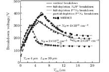
However, the increase of Tox will not increase the breakdown voltage absolutely. Figure 6 shows the influences of Tox on VB in different cases. At a very thin buried oxide layer, where there is a linear variation of breakdown voltage with Tox, and the slope of the curve of the breakdown voltage versus Tox is determined by Eq. (10). When Tox increases to the point where the vertical breakdown is higher than the lateral breakdown voltage, the breakdown location moves to the surface NdN+ junction, and VB is determined by Eq. (9). As Tox increases, the breakdown voltage reaches a peak and then decreases because the breakdown location moves to the P+ Nd junction. If the buried oxide layer is very thick, the drift region will be partially depleted when breakdown occurs, and the breakdown voltage is independent of Tox according to Eq. (4).
Fig. 6. Dependences of breakdown voltage on buried oxide thickness in different cases.
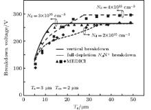
Figure 7 shows the calculated breakdown voltages each as a function of the drift region length, along with the MEDICI simulations. Breakdown occurs at the NdN+ junction with a very short drift region. When the drift region is long enough, it is hard for the lateral breakdown to occur. The constant breakdown voltage independent of Ld can be seen because of the vertical breakdown formulated by Eq. (10).
As figure 8 shows, the breakdown voltages are each plotted as a function of Nd for various values of Ts. When the SOI layer is very thin, a very high doping concentration in the drift region is adopted to obtain the maximum lateral breakdown voltage. As equations (10) and (12) show, if Nd is high enough, VBlat max will be lower than VBver and breakdown occurs only on the surface. For example, when Ts = 3.5 μ m, breakdown will go through three stages: lateral breakdown at the NdN+ junction for the full-depletion case, lateral breakdown at the P+ Nd junction for the full-depletion case, and lateral breakdown at the P+ Nd junction for the partial-depletion case. However, when Ts is very thick, the increase of Ts will rapidly improve the vertical breakdown voltage as shown in Eq. (10). As a result, the vertical breakdown voltage will be higher than VBlat max, and breakdown will also go through three stages. For example, when Ts = 28.5 μ m, the breakdown voltage as a function of Nd also presents three stages determined by Eqs. (9), (7), and (4) respectively. When Ts is moderate (for example Ts = 6 μ m or 12 μ m), breakdown goes through four stages. As figure 8 shows, the breakdown location moves from the PdN+ junction, to the Si– SiO2 interface to the P+ Nd junction with the increase of Nd. Therefore, the breakdown voltage is determined by Eqs. (9), (10), (7), and (4) respectively.
Fig. 8. Dependences of breakdown voltage on the doping concentration in the drift region in different cases.
4. RESURF criterion
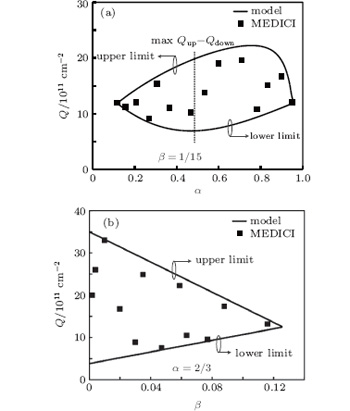
As shown in Figs. 5– 8, it is desirable that the device breakdown on the Si– SiO2 interface other than the surface benefits the improvement of the breakdown voltage. By substituting Eq. (10) into Eqs. (7) and (9), the upper and lower limit of the drift region doping dose are obtained as follows:
where α = Ts/Ld and β = Tox/Ld are the shape factors of the SOI layer and the buried oxide layer, respectively. Hereby, the RESURF criterion can be expressed as
According to Eq. (15), a theoretical window for optimizing the drift doping dose is derived and shown in Fig. 9. The numerical simulations by MEDICI fall within the window, thus demonstrating the validity of the model.
Fig. 9. Plots of impurity dose in the drift region versus shape factors for (a) SOI layer and (b) buried oxide layer.
During designing the lateral power device, it is targeted to acquire a large Qup– Qdown to realize the vertical breakdown. For the given α and β , a large Qup– Qdown represents a large process tolerance in the drift implantation. As figure 9(a) shows, when α is either very large or very small, the Qup– Qdown is relatively small. The vertices shown in the figure can be obtained by substituting Eqs. (13) and (14) into Eq. (14) as follows:
As shown in Fig. 9(b), when β is very small, the Qup– Qdown is relatively large. However, as figure 6 shows, a small β also means a low breakdown voltage. During designing a lateral power device, the trade-off between the process tolerance and the maximum breakdown voltage ought to be considered. As equation (16) shows, in order to obtain the maximum Qup– Qdown, α and β ought to follow the relationship:
5. Conclusion
A new simple 1D breakdown model for the SOI RESURF lateral power device is developed. We propose that the charges in the drift region are allocated to the lateral and vertical depletion regions along the diagonal of the sharing area. Thus, the lateral junction can be equivalent to a single side abrupt linear graded junction. Such an assumption gives a good explanation for the improvement in breakdown voltage of a RESURF structure when the drift region is fully or partially depleted. Finally, a new RESURF criterion is derived to provide the available guidance on optimizing the geometric parameters of SOI RESURF lateral power devices. The analytical model is verified by the good agreement between the modeling results and simulation results by the TCAD tools.
AppelsJ A and VaesH M1979Proceedings of the 25th Electron Devices MeetingDecember 3–51979, Washington D C, USA238[Cited within:2]
5
HunagY S and BaligaB J1991Proceedings of the 3rd International Symposium on Power Semiconductor Devices and ICsApril 22–241991, Baltimore, USA27[Cited within:3]
FanJ, ZhangB, LuoX R and LiZ J2010Proceedings of the 10th International Conference on Solid-State and Integrated Circuit TechnologyNovember 1–41991, Shanghai, China966[Cited within:2]
Abstract This paper is focused on the analysis and optimization of power N-type LDMOS (LDNMOS) transistors ( V BR > 120 V) with the purpose of being integrated in a new generation of Smart-Power technology based upon a 0.18 μm SOI-CMOS technology. The influence of some important design parameters such as the shallow trench isolation (STI) length ( L STI ), the N-well doping profile and the relative position of the N-well mask to the STI block are analyzed in terms of voltage capability ( V BR ), specific on-state resistance ( R on-sp ) and electrical safe-operating area (SOA) by means of Technology Computer-Aided Design (TCAD) numerical simulations. The evolution of the measured and simulated V BR as a function of the substrate (handle wafer) voltage (HWV) gives good physical insight of the optimal LDNMOS drift region design configuration. LDNMOS transistors with STI lengths partially covering the drift region length leads to better combined action of R on-sp / V BR trade-off and electrical SOA results.
... [1,2,14] Typically, the drift region is already fully depleted (Xver #cod#x003E ...
4
2004
0.0
0.0
... [3] Therefore, when #cod#x03B7 ...
... [3,4] ...
... [3,5,9,10] ...
... [3,4,5] Figures#cod#x00A0 ...
2
1979
0.0
0.0
... [3,4] ...
... [3,4,5] Figures#cod#x00A0 ...
3
1991
0.0
0.0
... [5,9,10] Although 2D models can effectively analyze the 2D electric field and potential distribution, mathematical expressions are very complicated and lacking in clear physical meaning ...
... [3,5,9,10] ...
... [3,4,5] Figures#cod#x00A0 ...
1
2005
1.482
0.0
... [6#cod#x2013 ...
2
2010
0.0
0.0
... 7] Silicon on insulator (SOI) technology avoids the adverse effect of substrate on the device via inserting a buried oxide (BOX) layer between the substrate and the SOI layer ...
... [7#cod#x2013 ...
1
2012
1.482
0.0
2
1995
1.482
0.0
... [5,9,10] Although 2D models can effectively analyze the 2D electric field and potential distribution, mathematical expressions are very complicated and lacking in clear physical meaning ...
... [3,5,9,10] ...
2
1996
0.0
0.0
... [5,9,10] Although 2D models can effectively analyze the 2D electric field and potential distribution, mathematical expressions are very complicated and lacking in clear physical meaning ...
... [3,5,9,10] ...
1
2012
1.137
0.0
1
1998
0.0
0.0
... 12] ...
1
2011
1.137
0.0
... [13#cod#x2013 ...
2
2006
0.912
0.0
... 14] Meanwhile, the breakdown mechanism of SOI RESURF is different from that of bulk silicon RESURF ...
... [1,2,14] Typically, the drift region is already fully depleted (Xver #cod#x003E ...
A new analytical model of high voltage silicon on insulator (SOI)thin film devices is proposed, and a formula of silicon criticalelectric field is derived as a function of silicon film thickness bysolving a 2D Poisson equation from an effective ionization rate,with a threshold energy taken into account for electron multiplying.Unlike a conventional silicon critical electric field that isconstant and independent of silicon film thickness, the proposedsilicon critical electric field increases sharply with silicon filmthickness decreasing especially in the case of thin films, and cancome to 141V/μm at a film thickness of 0.1μm which ismuch larger than the normal value of about 30V/μm. From theproposed formula of silicon critical electric field, the expressionsof dielectric layer electric field and vertical breakdown voltage(V B,V ) are obtained. Based on the model, an ultra thin filmcan be used to enhance dielectric layer electric field and soincrease vertical breakdown voltage for SOI devices because of itshigh silicon critical electric field, and with a dielectric layerthickness of 2μm the vertical breakdown voltages reach 852and 300V for the silicon film thicknesses of 0.1 and 5μm,respectively. In addition, a relation between dielectric layerthickness and silicon film thickness is obtained, indicating aminimum vertical breakdown voltage that should be avoided when anSOI device is designed. 2D simulated results and some experimentalresults are in good agreement with analytical results.
State Key Laboratory of Electronic Thin Films andIntegrated Devices, University of Electronic Science and Technologyof China,Chengdu 610054, China
A new analytical model of high voltage silicon on insulator (SOI)thin film devices is proposed, and a formula of silicon criticalelectric field is derived as a function of silicon film thickness bysolving a 2D Poisson equation from an effective ionization rate,with a threshold energy taken into account for electron multiplying.Unlike a conventional silicon critical electric field that isconstant and independent of silicon film thickness, the proposedsilicon critical electric field increases sharply with silicon filmthickness decreasing especially in the case of thin films, and cancome to 141V/μm at a film thickness of 0.1μm which ismuch larger than the normal value of about 30V/μm. From theproposed formula of silicon critical electric field, the expressionsof dielectric layer electric field and vertical breakdown voltage(V B,V ) are obtained. Based on the model, an ultra thin filmcan be used to enhance dielectric layer electric field and soincrease vertical breakdown voltage for SOI devices because of itshigh silicon critical electric field, and with a dielectric layerthickness of 2μm the vertical breakdown voltages reach 852and 300V for the silicon film thicknesses of 0.1 and 5μm,respectively. In addition, a relation between dielectric layerthickness and silicon film thickness is obtained, indicating aminimum vertical breakdown voltage that should be avoided when anSOI device is designed. 2D simulated results and some experimentalresults are in good agreement with analytical results.
Effects of an ultra-strong magnetic field on electron capture rates for Co-55 are analyzed in the nuclear shell model and under the Landau energy levels quantized approximation in the ultra-strong magnetic field, and the electron capture rates on 10 abundant iron group nuclei at the surface of a magnetar are given. The results show that electron capture rates on Co-55 are increased greatly in the ultra-strong magnetic field, by about 3 orders of magnitude generally. These conclusions play an important role in future study of the evolution of magnetars.
Du Jun 1 ;Li Ping-Ping 1 ;Luo Xia 1,2 ;
Effects of ultra-strong magnetic field on electron capture rates for 55 Co are analyzed in the nuclear shell model and under the Landau energy levels quantized approximation in the ultra-strong magnetic field, and the electron capture rates on 10 abundant iron group nuclei at the surface of magnetar are given. The results show that electron capture rates on 55 Co are increased greatly in the ultra-strong magnetic field, by about 3 orders of magnitude generally. These conclusions play an important role in future studying the evolution of magnetar.
... 16] The study on the breakdown model is helpful to ascertaining the breakdown mechanism and providing guidance on structural optimization design ...
One-dimensional breakdown voltage model of SOI RESURF lateral power device based on lateral linearly graded approximation*
[Zhang Jun, Guo Yu-Feng†, Xu Yue, Lin Hong, Yang Hui, Hong Yang, Yao Jia-Fei]


 , Xu Yue, Lin Hong, Yang Hui, Hong Yang, Yao Jia-Fei]