


Effects of annealing temperature on shape transformation and optical properties of germanium quantum dots*
[Samavati Alirezaa)†  , Othaman Z.
a) , Ghoshal S. K.b) , Mustafa M. K.c) ]
, Othaman Z.|
|


Corresponding author. E-mail: alireza.samavati@yahoo.com
Project supported by Ibnu Sina Institute for Fundamental Science Study, Universiti Teknologi Malaysia through Vote Q.J130000.2526.02H94, O5 and Postdoctoral Research Grant.
The influences of thermal annealing on the structural and optical features of radio frequency (rf) magnetron sputtered self-assembled Ge quantum dots (QDs) on Si (100) are investigated. Preferentially oriented structures of Ge along the (220) and (111) directions together with peak shift and reduced strain (4.9% to 2.7%) due to post-annealing at 650 °C are discerned from x-ray differaction (XRD) measurement. Atomic force microscopy (AFM) images for both pre-annealed and post-annealed (650 °C) samples reveal pyramidal-shaped QDs (density ∼ 0.26× 1011 cm−2) and dome-shape morphologies with relatively high density ∼ 0.92 × 1011 cm−2, respectively. This shape transformation is attributed to the mechanism of inter-diffusion of Si in Ge interfacial intermixing and strain non-uniformity. The annealing temperature assisted QDs structural evolution is explained using the theory of nucleation and growth kinetics where free energy minimization plays a pivotal role. The observed red-shift ∼ 0.05 eV in addition to the narrowing of the photoluminescence peaks results from thermal annealing, and is related to the effect of quantum confinement. Furthermore, the appearance of a blue-violet emission peak is ascribed to the recombination of the localized electrons in the Ge-QDs/SiO2 or GeO x and holes in the ground state of Ge dots. Raman spectra of both samples exhibit an intense Ge–Ge optical phonon mode which shifts towards higher frequency compared with those of the bulk counterpart. An experimental Raman profile is fitted to the models of phonon confinement and size distribution combined with phonon confinement to estimate the mean dot sizes. A correlation between thermal annealing and modifications of the structural and optical behavior of Ge QDs is established. Tunable growth of Ge QDs with superior properties suitable for optoelectronic applications is demonstrated.
Self-organization of strained coherent QDs via the well-known Stranski– Krastonov (SK) growth is a subject of unlimited scientific and practical significance.[1– 3] Charge carriers in QDs are confined in all three spatial dimensions, which results in energy state distribution and makes them highly favorable for device applications.[4, 5] For instance, Ge/Si QDs are interesting for integrated optoelectronic systems.[6] In the bulk form, the indirect band gaps of bulk Si and Ge can be problematic for some applications. On the other hand, the electronic states of Ge/Si QDs can be engineered by optimizing the growth parameters which govern their sizes and shapes.[7] QDs having different shapes have been observed in a number of material systems.[8, 9] Practically, for tuning the band structure of QDs, shape could be used as a valuable additional degree of freedom. Furthermore, the optical and electrical properties are influenced by size, strain, and chemical composition. Recently, extensive experimental studies on the structure and composition of Ge/Si QDs have been carried out.[10– 13] However, the mechanism of shape transformation and the exact correlation between shape conversion and size evolution during the growth of Ge QDs deserve further investigation. Moreover, their effects on optical behavior and structural evolution are far from being understood.
We demonstrate the annealing temperature-dependent surface morphology and optical properties of self-assembled Ge/Si (100) QDs grown by rf magnetron sputtering. Experimental observation is supported by the theory of growth kinetics and phonon confinement model. The QD growth as well as shape transformation is strongly guided by the inhomogeneity of strain mismatch within the structure. A quantitative analysis of the strain effects is emphasized through the Williamson– Hall model. Samples are thoroughly characterized via x-ray diffraction (XRD), atomic force microscopy (AFM), energy dispersive x-ray spectroscopy (EDX), room temperature photoluminescence (PL), and Raman spectroscopy.
Ge QDs are deposited on p-type Si (100) wafers of resistivity ρ = 5 Ω · cm– 10 Ω · cm. Prior to deposition, the substrate surface is treated to remove native oxide and to desorb water. The standard cleaning process is carried out in which Si (100) is first etched with hydrofluoric acid (HF 5% ) for 2 min and then cleaned ultrasonically in chromatic acid solution for 20 min followed by deionized water. The sputtering system (HVC Penta Vacuum) features a 1-m3 volume deposition chamber, evacuated to a base pressure of 6 × 10− 6 Torr (1 Torr = 1.33322 × 10² Pa) by turbo pumping. Ultrapure Ar (99.9999% ) plasma is activated by the rf-pulsed generator (13.56 MHz). Sputtering is performed from a crystalline Ge target (99.999% purity), bonded onto a circuit magnetron cathode in vertical configuration. The growth process is undertaken under the condition of 10-sccm Ar flow, 400-° C substrate temperature, 300-s deposition time, and 100-W rf power. The Ge target is pre-sputtered for 120 s before deposition. A post-growth annealing step is applied to a subset of samples in a rapid thermal processing oven (Anneal sys, AS-One 150) in nitrogen (N2) ambient at 300, 450, and 650 ° C for 2 min and then cooled down spontaneously.
The morphologies and structural analyses of samples are characterized using an atomic force microscope (SPI3800) built by Seiko Instrument Inc. (SII) and x-ray diffraction (Bruker D8 Advance Diffractometer) using Cu-Kα 1 radiations (1.540 Å ) at 40 kV and 100 mA. The scanning range of 2θ is varied from 0° to 40° . A slow speed of scanning ∼ 1.2° /min with a resolution of 0.011° is employed. The elemental composition of the sample is analyzed through an energy dispersive x-ray diffractometer (EDX) attached to FESEM, JEOL, JSM-6701F. The room temperature photoluminescence measurement (Perkin Elmer Ls 55 Luminescence Spectrometer) is carried out in the visible region using an excitation wavelength of 239 nm. Raman spectroscopy is performed using a spectrum GX (NIR, FT- Raman) system with a Nd crystal laser source having a spot size of 1 μ m.
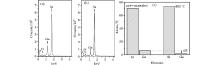
The energy dispersive x-ray (EDX) spectra for the edge spots of samples pre-annealed and annealed at 650 ° C are shown in Fig. 1, and clearly reveal the presence of Ge, Si, O, and C elements. The appearance of Ge peaks exhibits the Ge QDs, which is inconsistent with the AFM result. The occurrence of the carbon (C) signal is due to the supportive carbon tape attached to the sample holder, while the oxygen (O) peak originates from the surface passivation of the dangling bonds and subsequent formation of SiO2 and GeOx defects during growth and sample transformation to analysis equipments. The atomic percentages (Fig. 1(c)) are calculated using EDX spectra and reveal that upon annealing, the amount of Ge in the edge of dots decreases, which is attributed to a higher level of interfacial intermixing of Ge with the Si substrate.
 | Fig. 1. EDX spectra of pre-annealed (a), post-annealed sample at 650 ° C (b), and corresponding atomic percentages of the edge spot (c). |
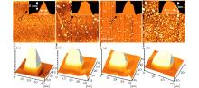
Two-dimensional (2D) and corresponding high magnification three-dimensional (3D) typical AFM images of selected dots (inset) are illustrated in Fig. 2. Two kinds of Ge nanocrystal morphologies are identified, including the square base pyramid-like dots for pre-annealed sample with average height ∼ 9 nm and width ∼ 21 nm and dome-like dots for the sample annealed at 650 ° C (Fig. 2(d)) with average height ∼ 5 nm and width ∼ 29 nm. It is important to note that the determined size of QD using AFM observation is slightly overestimated because of the tip artifact.
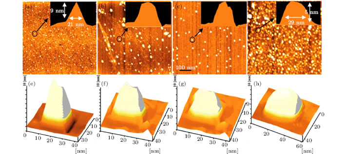 | Fig. 2. Two-dimensional AFM images of Ge QDs on Si substrates, pre-annealed (a) annealed at 300 ° C (b), 450 ° C (c), and 650 ° C (d). Insets show the sizes and shapes of selected dots. Transition stage from pyramidal for pre-annealed (e) to dome-like structure post-annealed at 650 ° C (h) is shown at high magnification 3D images of the selected QDs. |
At the pre-annealed sample, most of the Ge atoms are contained in the smaller pyramids as entropy attempts to maximize the number of dots on the surface. At the annealing temperature below 650 ° C, low-adatom mobility often impedes the formation of a nucleation center on the surface and may kinetically restrict the dot formation, which leads to the appearance of lower number densities for these samples. By the heating treatment process, the shape of pyramid-like QDs gradually changes into the dome-like shape. The dot distributions coarsen during annealing over a portion of temperature range.
The integrated volume of the QDs increases during annealing as some of the Ge atoms move from the wetting layer into the QDs. The transformation from one shape to another complicates the coarsening process. Both pyramids and domes are in equilibrium structures. Therefore, the observed coarsening represents the evolution toward the lowest-energy configuration of the system consistent with the temperature going up. The process responsible for coarsening is Ostwald ripening. Consequently, the free energy of the dots decreases monotonically with increasing the QD size. The eventual slowing of the coarsening could be caused by a kinetic barrier for an atom to attach to the mature domes. Diffusion of Si from the substrate into the Ge QDs during annealing at higher temperatures changes the energetically favorable shape of a given sized QD. At 650 ° C the solid-state diffusion coefficient of Ge in unstrained Si is very small (∼ 10− 26 m2· s− 1) while the solid-state diffusion coefficient of Si in unstrained Ge is much larger (∼ 3 × 10− 21 m2· s− 1).[14] Therefore, by annealing preferably the Si substrate, the inter-diffuse in Ge wetting layers and QDs is caused to reduce the strain as confirmed in the Williamson– Hall plot in Fig. 7.
The schematic diagrams for shape evolution and interfacial intermixing procedure are illustrated in Fig. 3. Strain relaxation could increase the diffusion length by ∼ 5× for annealed samples.[15] Inter-diffusion is non-uniform across the dots which results in non-uniformity of intermixing. Therefore, the strain at the interface between the Si substrate and the Ge dots is highly inhomogeneous, being much greater near the center than near the edges. The lower strain near the edge suggests higher intermixing and it is responsible for the observed shape evolution.
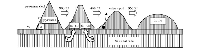 | Fig. 3. Schematic representation of the QD transition mechanism. Si substrate diffuses into the perimeter of pyramidal Ge dots forming an Si– Ge composition. It causes misfit reduction and non-uniformity of strain across the dots leading to the formation of domes at 650 ° C. EDX is recorded at the edge spot. |
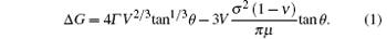
The increase in size as well as the number density for the post annealed (650 ° C) sample can be explained by nucleation and growth kinetics processes. The thermodynamic stability and the free energy minimization are considered. Formation of 3D QDs causes lateral relaxation of the lattice planes, which are compressed in the bulk of the film thereby reducing the elastic energy stored in the film. However, the dots also cost additional surface energy so the simplest model for the QD formation energy as a function of dot volume V is given by[16]
Here θ is the contact angle (Fig. 3), σ is the misfit stress, μ is the shear modulus (67 GPa), ν is Poisson’ s ratio (0.28) for Ge, and Γ is the surface energy and given by

where γ f and γ s are the respective facet and surface energies, which are depicted in Fig. 3.
The first term on the right-hand side in the free energy expression above is proportional to the surface area and signifies the additional surface energy created. However, the second term corresponds to the elastic energy released and is proportional to the dot volume. For sufficiently large dots, the elastic term eventually dominates. Although it is necessary to overcome the activation barrier in order to form stable dots, this barrier energy which is a strong function of misfit stress σ follows[16]
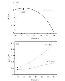
Truly, the overall morphology of dots is driven by the details of the growth kinetics. The dot size-dependent energy variation is presented in Fig. 4(a). Initially, the increase in energy associated with the growth of a facial-dot is caused by the stress concentration at its base. Consequently, the formation of the face is rapid for sufficiently large coverage, which is due to the domination of released elastic energy. Clearly, an activation barrier must be overcome to nucleate a strained facet. This barrier increases as dot size and misfit stress augment, which is shown in Fig. 4(b).
 | Fig. 4. (a) Variarion of energy change with the size of QDs (a), and (b) variations of activation barrier Δ G* with QDs size for two misfits (ε = 0.03 and 0.05) based on the Williamson– Hall plot. |
The QD nucleation rate is governed by

where the pre-factor DL incorporates the rate-limiting step involving the transport and attachment of mass to the dot, kB is the Boltzmann constant, and T is the temperature. The exponential dependence of the growth rate on barrier energy confirms that the faster nucleation with larger density in the post-annealed sample results from a lower energy barrier and weaker stress misfit. Furthermore, this self-limiting behavior, which is significant at higher misfits, may result in a considerable reduction in growth rate (number density) even for small dots in a pre-annealed sample. The observed increases in nucleation rate and dot size due to annealing strongly support the theoretical explanations.
The different dot shapes in the AFM micrograph are quantified by measuring the diameters and heights of all dots. Figure 5 shows scatter plots of Ge QDs width and aspect ratio (height/width) each as a function of percentage of QDs, derived from the data set depicted in Fig. 2, excluding the very large dots. Decreasing of the aspect ratio by increasing the dot width via annealing indicates the shape transition of dots.
 | Fig. 5. Width and aspect ratio distributions of QDs for pre-annealed (a) and annealed at 300 ° C (b), 450 ° C (c), and 650 ° C (d). |
Hetero-epitaxial self-assembly leads to remarkably narrow dot size distributions. There are different contributions to explain the size distribution of Ge QDs. Dot growth is kinetically limited and larger dots should grow more slowly than smaller ones. This would allow smaller dots to form and cause the size distribution to narrow.[17, 18] Other models assume the existence of an equilibrium dot size for a specific combination of material parameters, [19] which results in stable and non-ripening size distribution. Another perspective is that the chemical potential of QDs falls monotonically with size and allows the Ostwald ripening process.[20] In view of the above mechanisms, by increasing the annealing temperature the size distribution of QDs becomes narrower.
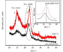
Figure 6 illustrates the XRD patterns of samples pre-annealed and post-annealed at 650 ° C, in which the Ge (220) peak is marked by a dash– dotted loop and expanded in the inset. The vertical dotted lines indicate the peak positions and shift corresponding to the pre-annealed pattern. The strain field between Ge nanocrystallites and the surrounding matrix changes the lattice parameters by varying the inter-spacing of the planes. Inter-diffusion of Si into the wetting layer and dots causes the strain and lattice parameter to change. The observed shift in the XRD spectra for the Ge (220) peak corresponding to the 650-° C sample confirms that a Si– Ge alloy forms during annealing.
 | Fig. 6. XRD spectra from samples pre-annealed and post annealed at 650 ° C. Inset shows the shift for Ge (220) peak. |
The strain field between Ge nanocrystallites and the surrounding matrix changes the lattice parameters by varying the interspacing of the planes. The broadening of the XRD peaks is attributed mainly to the presence of various crystallite sizes, microstrain and instrumental effects. The broadening caused by the effects of strain can be determined by the Williamson– Hall plot (β cosθ versus sinθ ) shown in Fig. 7. This plot is generated corresponding to the XRD peaks 1 and 2 whose details are displayed in the inset. Here, β is the full width at half maximum (FWHM). A linear relation between β cosθ and sinθ suggests the contribution of strain to the broadening of the XRD peak. On the other hand, if the contribution to broadening appears only due to the size variation then β cosθ would remain constant.[21]
 | Fig. 7. Williamson– Hall plot of samples pre-annealed and post annealed at 650 ° C. |
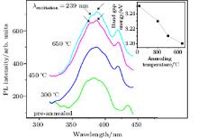
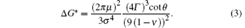
The observed dot shape transition and size equalization are also apparent in the optical spectra. Figure 8 shows PL spectra (taken at room temperature) for all samples. For the pre-annealed sample, a single peak at ∼ 3.25 eV accompanied by a weak shoulder at ∼ 2.85 eV can be seen. At 300 ° C, the peak moves to ∼ 3.23 eV and broadens with a FWHM of ∼ 0.33 eV. This is consistent with the initial broadening in dot lateral size and, perhaps more importantly, variation in dot height. At 450 ° C, the intense peak is deconvoluted into two peaks which are shown by arrows at 3.27 eV and 3.21 eV, corresponding to the emissions that originate from two distinct mechanisms explained using Fig. 9. The near band-edge transition of free exciton through an exciton– exciton collision process within dots and two different energy levels of defect may contribute to the appearance of these two nearby peaks.
 | Fig. 8. Room temperature PL spectra. Inset indicates the shift in the band gap. |
 | Fig. 9. Schematic band structures of Ge-dot/SiO2 and GeOx defects. The energies of 1.17 eV and 0.66 eV correspond to the band gaps of bulk Si and Ge respectively. |
At 650 ° C, the peak moves to 3.20 eV and narrows to a FWHM of ∼ 0.25 eV. In comparison with the pre-annealed sample, such a smaller FWHM is mostly attributed to the simultaneous dot shape stabilization and size equalization. Following the Ge-QDs/SiO2 or GeOx interface model[22] (Fig. 9), the origin of the blue-violet peak (3.20 eV) in the PL spectra is explained. In this case, the electrons from the conduction band of the Ge or Si do not participate in the radiative recombination processes. Indeed, the localized electrons in the radiative defect states at the Ge-dot/SiO2 or GeOx interfaces are responsible for the emission peak. Min et al.[23] and Takeoka et al.[24] proposed similar mechanisms for radiative recombination on the ion-implanted Ge in SiO2 and the rf co-sputtered Ge and SiO2 nanostructures, respectively. The observed red shift ∼ 0.05 eV in the PL peak for a post annealed sample at 650 ° C compared with pre-annealed one is related to the increase of the average size of QDs.
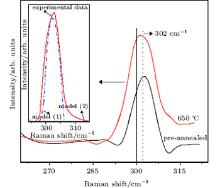
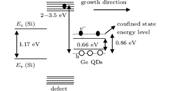
The Raman spectra of pre- and post-annealed (650 ° C) samples are shown in Fig. 10, in which the inset shows the peak of Ge– Ge optical phonon for the annealed sample. The Raman spectra contain the information about the vibration (phonon modes) of molecule or crystal used as a fingerprint for identifying species and crystal phases. The optical phonon position matching to the bulk crystalline Ge is shown by the vertical solid line at 300 cm− 1. Some phonons and vibrational modes are restricted in the low dimensional system upon nanosizing. This restriction is referred to as quantization. Nnaosizing displays different behaviors on Raman spectra such as changes in the symmetry of the vibration peaks, shift to different energies, and variation in the peak intensity, which vanishes or is even enhanced.
 | Fig. 10. Frequency positions of the Ge– Ge optical phonons which are shifted slightly towards higher frequencies with respect to their bulk value. Inset: shows the Ge– Ge optical phonon annealed at 650 ° C fitted with theory models. |
The Raman spectra indicate that the first-order transverse optical (TO) phonon mode of Ge QDs occurs at ∼ 302 cm− 1 and it is in conformity with the result of Kartopu et al.[25] A shift for the strongest Raman peak at ∼ 302 cm− 1 corresponding to the Ge– Ge phonon mode towards higher frequency with respect to the bulk crystalline Ge, which is expected to occur at ∼ 300 cm− 1, is ascribed to the competitive effect between strain and phonon confinement. Based on a simple linear chain model, the optical phonon branches of the bulk Ge are quadratic and nearly flat in the Brillouin zone center (k ∼ 0). In an infinite crystal, the wave vector for restricted phonon vibration is given by mπ /d with m being an integer and d the diameter of the nanocrystal.[26] Therefore, a shift of optical phonons towards a lower frequency is expected to occur due to the spatial limitations of QDs. A shift of ∼ 2 cm− 1 toward the lower frequency for dots with very small heights ∼ 1.5 nm– 2 nm due to phonon confinement was observed by Liu et al.[27] Therefore, the strain plays a predominant role in shifting the peak towards the higher frequency. The lattice mismatch between Si and Ge leads to a compressive strain on the dots in the lateral directions. For fully strained pure Ge on Si, the calculated value of ω is 317.4 cm− 1, [28] and the corresponding experimental value is 302 cm− 1 (Fig. 10). This dissimilarity in the theoretical and experimental values suggests that the dots in the samples are not completely strained as supposed in the theory that is confirmed in the Williamson– Hall plot (Fig. 7). Due to the microscopic mechanisms such as the presence of threading dislocations and the Ge– Si atomic intermixing, the strain relaxation of dots increases. The signature of the intermixing is evidenced as the Ge– Si peak at around 400 cm− 1 in full scale Raman spectra, which is not shown here.
For the investigation of the size distribution effect and the estimation of dot size, the Raman spectra of the annealed sample are fitted by two theoretical models. which were explained in our recent research.[29] The experimental Raman spectrum of Ge-Ge phonon vibration for the annealed sample is shown by a solid curve in the inset of Fig. 10 and is fitted with the models Eq. (1) (lower dashed curve) and Eq. (3) (middle dotted curve) in which the models (1) and (3) are attributed to the phonon confinement and the phonon confinement combined with the size distribution model respectively. The best fit is achieved by adjusting the value of L and assuming each of the QDs to have a spherical shape. It is clear that the dotted line generated using a Gaussian distribution is closer to the experimental curve than the dashed line and is in conformity with the research result of Fauchett and Campbell.[30] The calculated size of the Ge QDs using models (1) and (3) are ∼ 9 nm and ∼ 12 nm respectively.
The influence of thermal annealing on shape transformation of self-assembled Ge/Si (100) QDs prepared by rf magnetron sputtering is demonstrated. The annealing temperature driven variations in shape and size of Ge/Si QDs displayed by the AFM images are explained in terms of the growth kinetic model and involved strain relaxation mechanism. Post-annealing at 650 ° C results in: 1) an increase in the volume of dots due to moving Ge atoms from the wetting layer to the dots, 2) inter-diffusion of the Si substrate in the Ge wetting layer and QDs causing the interfacial intermixing and non-uniformity of strain. These two phenomena are mainly responsible for the change from a pyramidal to a dome-like shape. Annealing assisted (650 ° C) reduction in strain from 4.9% to 2.7% is explained through a Williamson– Hall plot using two intense XRD peaks corresponding to the preferred growth along Ge (111) and Ge (220) planes. Furthermore, the observed shifts of these XRD peaks and the variation in the lattice constant of Ge nanocrystallites are attributed to the strain field between dots and its surrounding matrix. The appearance of a blue-violet band in the room temperature PL spectra is ascribed to the electron– hole recombination from defects excited state to the ground-state belonging to Ge QDs. Post annealing (650 ° C) mediated red shift ∼ 0.05 eV in the PL peak is attributed to the effect of quantum confinement. The occurrence of an intense Ge– Ge optical phonon mode accompanied by a shift towards higher frequency in the Raman spectra is explained using two different models. The model with Gaussian size distributions plus phonon confinement is found to fit better to the experimental Raman profile. The admirable features of the results suggest that our careful methods of achieving high-quality Ge/Si QDs with controlled shape and size may contribute to the development of efficient optoelectronic materials.
| 1 |
|
| 2 |
|
| 3 |
|
| 4 |
|
| 5 |
|
| 6 |
|
| 7 |
|
| 8 |
|
| 9 |
|
| 10 |
|
| 11 |
|
| 12 |
|
| 13 |
|
| 14 |
|
| 15 |
|
| 16 |
|
| 17 |
|
| 18 |
|
| 19 |
|
| 20 |
|
| 21 |
|
| 22 |
|
| 23 |
|
| 24 |
|
| 25 |
|
| 26 |
|
| 27 |
|
| 28 |
|
| 29 |
|
| 30 |
|