Wang Jun†, Hu Hai-Yang, Deng Can, He Yun-Rui, Wang Qi, Duan Xiao-Feng, Huang Yong-Qing, Ren Xiao-Min. Defect reduction in GaAs/Si film with InAs quantum-dot dislocation filter grown by metalorganic chemical vapor deposition* . Chinese Physics B, 2014, 24(2): 028101
Permissions
Defect reduction in GaAs/Si film with InAs quantum-dot dislocation filter grown by metalorganic chemical vapor deposition*
Wang Jun†, Hu Hai-Yang, Deng Can, He Yun-Rui, Wang Qi, Duan Xiao-Feng, Huang Yong-Qing, Ren Xiao-Min
Institute of Information Photonics and Optical Communications, Beijing University of Posts and Telecommunications (BUPT), State Key Laboratory of Information Photonics and Optical Communications (BUPT), Beijing 100876, China
Project supported by the Fundamental Research Funds for the Central Universities, China (Grant No. 2013RC1205) and the National Basic Research Program of China (Grant No. 2010CB327601).
Abstract
Abstract
The growth of GaAs epilayers on silicon substrates with multiple layers of InAs quantum dots (QDs) as dislocation filters by metalorganic chemical vapor deposition (MOCVD) is investigated in detail. The growth conditions of single and multiple layers of QDs used as dislocation filters in GaAs/Si epilayers are optimized. It is found that the insertion of a five-layer InAs QDs into the GaAs buffer layer effectively reduces the dislocation density of GaAs/Si film. Compared with the dislocation density of 5×107 cm−2 in the GaAs/Si sample without QDs, a density of 2×106 cm−2 is achieved in the sample with QD dislocation filters.
High-quality GaAs/Si epilayers combine the advantages of both Si and GaAs materials, and can be used in many important fields. Firstly, monolithic integration chip with the GaAs-based optoelectronic and Si-based microelectronic devices has been realized.[1, 2] Secondly, due to the brittleness and higher cost of GaAs wafers, GaAs/Si epilayers could replace GaAs substrates for applications in high-speed microelectronic[3– 5] and optoelectronic devices.[6– 10] Finally, optoelectronic integrated circuits on silicon chips attract ever-increasing attention in the need of high-bandwidth optical interconnects.[11– 13]
Due to the large differences in lattice constant and thermal expansion coefficient between GaAs and Si, and the difference between their polar/non-polar surface incompatibilities, the density of dislocations in the GaAs/Si epilayer is up to 108 cm− 2– 109 cm− 2.[13, 14] In order to improve the crystalline quality, various defect reduction methods have been proposed in the past two decades, such as the two-step growth, thermal cycle annealing, strained-layer superlattices (SLS), and patterned substrates.[15– 22]
According to dislocation theory, the strain field can bend dislocations, and result in their interaction or propagation toward wafer edges. Owing to the fact that the strain field around quantum dots (QDs) is much stronger than that of SLS, the built-in strain field of QD is recently introduced into epilayers to impede or bend threading dislocations generated at large misfit interfaces. When a threading dislocation propagates close to a quantum dot, a very strong Peach– Koehlor force will bend the dislocation energetically because the strain energy released is greater than the dislocation self-energy.[23, 24]
Through the insertion of a set of multiple quantum-dot layers into a buffer layer, Huang et al.[23] effectively reduced the dislocation density from ∼ 1010 cm− 2 to ∼ 3 × 107 cm− 2 in the GaN epilayer grown by molecular beam epitaxy (MBE) on a sapphire substrate. By using multiple layers of In(Ga)As/GaAs QDs grown by MBE as a dislocation filter to impede the propagation of dislocation in the GaAs/Si epilayer, an In0.5Ga0.5As/GaAs QD laser structure was grown on silicon, and the laser device was fabricated. The laser exhibited a threshold current density of 900 A/cm2 at 273 K, a high characteristic temperature of 278 K in the temperature range 5 ° C– 85 ° C, and an output slope efficiency of 0.4 W/A.[24, 25]
Although thick GaAs/Si epilayers have great advantages to grow by metalorganic chemical vapor deposition (MOCVD) technology, seldom has work been reported to study quantum dot layers used as dislocation filters in GaAs/Si epilayers grown by MOCVD.
In our previous investigations, the two-step growth of GaAs/Si epilayers[15– 17] and InAs/GaAs QDs on GaAs substrates, [26] have been studied in detail by MOCVD. In the present paper, based on our typical MOCVD-growth conditions of InAs QDs on GaAs substrates, the process parameters of growth conditions for a single layer of InAs QDs on a Si substrate are explored and optimized by combining with the two-step growth of GaAs layers on Si. Then, based on the growth conditions of a single quantum dot layer, growth conditions for multiple InAs quantum dot layers on Si substrates are determined. Finally, by using multiple layers of InAs QDs as dislocation filters, the effect of improving the crystalline quality of GaAs/Si epilayers is studied.
2. Experimental procedures
The growth of InAs QDs on GaAs/Si epilayers is carried out in a Thomas Swan 3× 2-inch (1 inch = 2.54 cm) close-coupled showerhead MOCVD system. The carrier gas is pd-cell purified hydrogen, and high-purity trimethylgallium (TMGa), trimethylindium (TMIn), and arsine are used as source materials. The 2-inch (100)-oriented Si wafers with 4° -misorientation toward the [011] direction are used as the substrates.
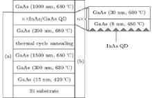
The detailed experimental procedure and sample structures are shown in Fig. 1. After chemical cleaning, the Si wafers are loaded into the reactor chamber of the MOCVD system, and baked at 220 ° C for 30 min, and then arsenic is passivated at 750 ° C for 15 min in an arsine and hydrogen ambient. Afterwards, a two-step growth process is performed to deposit the GaAs buffer layer. The temperature is first reduced to 420 ° C for growing the low-temperature GaAs nucleation layer with a thickness of 15 nm, then a moderate-temperature (630 ° C) and a high-temperature (680 ° C) GaAs layer with thickness values of 300 nm and 1500 nm are grown on the nucleation layer in sequence. After growing the buffer layer, a thermal cycle annealing is performed between 350 ° C and 750 ° C in the arsine and hydrogen ambient three times. Subsequently, a GaAs layer with a thickness of 200 nm is grown at 680 ° C. For the nucleation layer, the molar flow rates of TMGa and arsine are 2.7× 10− 5 mol/min and 6.7× 10− 3 mol/min. For the moderate- and high-temperature GaAs layers, the molar flow rates of TMGa and arsine are 4.0× 10− 5 mol/min and 2.7× 10− 3 mol/min respectively, and the growth rate is 36.0 nm/min.
Fig. 1. Schematic diagrams of the growth process for GaAs/Si samples with InAs QDs serving as dislocation filters.
The epilayer structure shown in Fig. 1(a) is used to adjust and optimize the growth conditions of InAs QDs. For multiple InAs quantum dot layers, each layer structure includes an InAs quantum dot layer, an 8-nm GaAs cap layer, and a 30-nm GaAs space layer as shown in Fig. 1.
Based on our previous growth conditions for InAs/GaAs QDs on a GaAs substrate, the molar flow rates of TMIn and arsine are 8.6× 10− 7 mol/min and 4.9× 10− 6 mol/min, and the growth temperature is 480 ° C for the InAs quantum dot layer. For the GaAs cap layer, the molar flow rates of TMGa and arsine are 4.0× 10− 5 mol/min and 2.7× 10− 3 mol/min, and the growth temperature and growth rate are 480 ° C and 3.0 nm/min, respectively. For the space layer, the molar flow rates of TMGa and arsine are the same as for the cap layer, and the growth rate is 36.0 nm/min at a growth temperature of 600 ° C. The reactor pressure is 100 Torr (1 Torr = 1.33322× 10² Pa) for the whole growth process of samples.
When adjusting the growth conditions for QDs, the surface quantum dot layer is uncapped for observing its surface morphology. The growth process and the detailed structure of GaAs/Si epilayers with QDs as dislocation filters are shown in Fig. 1(b).
3. Optimum growth conditions for InAs QDs on Si
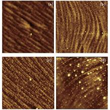
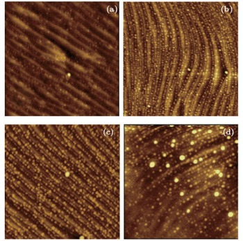
According to our experience in growing the InAs QDs on GaAs substrates, the nominal thickness (NT) is more sensitive to the surface morphology of QDs. Hence, we mainly optimize the NT of InAs as the growth parameter of InAs QDs on a Si substrate. The other growth conditions are as follows: the growth temperate and growth rate are 480 ° C and 0.036 ML/s respectively, and the V/III ratio is 6. The InAs QDs with different NT values of 2.16 ML, 2.34 ML, 2.52 ML, and 2.88 ML are grown on Si substrates by MOCVD. After growing, surface morphological characteristics of the samples are measured by atomic force microscopy (AFM) and the results are shown in Fig. 2.
Fig. 2. AFM images (1 μ m× 1 μ m) of the single layer QD sample with different nominal thickness values of (a) 2.16 ML, (b) 2.34 ML, (c) 2.52 ML, and (d) 2.88 ML.
As seen from Fig. 2, for the InAs deposition of NT of 2.16 ML, QDs of low density are distributed sporadically on the atomic steps. When the NT increases to 2.34 ML, the density of QDs increases, and their size and in-plane distribution become homogeneous. For the NT of 2.52 ML, the dot density of QDs increases, and big clusters begin to occur. When the NT increase to 2.88 ML, the size of QDs become more nonuniform, and the phenomenon of clusters becomes serious. Owing to lattice relaxation in these big clusters, dislocations can be generated in the larger QDs themselves. Therefore, the optimized NT of InAs is chosen to be 2.34 ML in the next experiments.
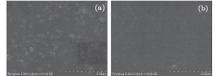
The effect of the QD dislocation filter depends strongly on the number of dot layers. For the dislocation filter with less dot layers, the ability to bend dislocations is weak, while for the dislocation filter with too many dot layers, the quality of QDs should deteriorate due to the formation of big relaxed QDs, and the crystalline quality of GaAs/Si epilayers decreases greatly. Especially for the MOCVD growth process, big clusters can be generated easily. In order to optimize the number of dot layers, the three- and five-layer QDs are grown with an NT of 2.34 ML. The surface morphological characteristics of both samples are shown in Fig. 3.
Fig. 3. AFM images (1 μ m× 1 μ m) of the samples with (a) three-dot layers and (b) five-dot layers.
As can be seen from Fig. 3, the size of dots is homogenous in the sample of three-layer QDs, and the phenomenon of big clusters hardly occurs. For the five-layer QDs, the dot density increases obviously. The size of dots becomes larger, but few of the big clusters occur. Since the more dot layers, the larger strain stress can be accumulated, the phenomenon of big clusters becomes serious, and those clusters should relax and generate dislocations. Taking account of the effects of both the layer number and surface morphology according to the results, the five-layer QDs are determined to be used as the optimized dislocation filters.
4. Multiple dot layers serving as dislocation filters in GaAs/Si epilayers
Using five-layer QDs as dislocation filters, the sample of GaAs/Si epilayers is grown by MOCVD according to the growth process and the detailed structure as shown in Fig. 1(b). That is, after growing the dislocation filter structures, another GaAs layer with a thickness of 1000 nm is grown, and the growth conditions are similar to those of the high-temperature GaAs layer. For comparison, another sample of GaAs/Si epilayers without a dot dislocation filter is also fabricated under the same growth conditions. Both samples display smooth mirror-like surfaces after having been grown.
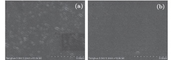
The etch pit densities (EPDs) of the two samples are measured by scanning electric microscopy (SEM) after the samples have been etched by molten KOH with an etching depth of about 300 nm. The results of the sample without and with QDs are shown in Figs. 4(a) and 4(b). The dense etch pits hardly allow us to reliably count the pit density in Fig. 4(a), while a few pits occur in Fig. 4(b). As can be seen, the EPD of the sample without QDs is greater than that with QDs. The dislocation density can be estimated from Fig. 4(b) to be 2× 106 cm− 2 for the sample with QDs, while for the sample without QDs, it is infeasible to estimate the dislocation density from Fig. 4(a), whose dislocation density is measured to be 5× 107 cm− 2 by transmission electron microscopy (TEM) instead. That is, the dislocation density of the sample of GaAs/Si epilayers can be reduced by more than one order of magnitude through using QDs as dislocation filters.
Fig. 4. SEM images of etched surfaces of the GaAs/Si samples (a) without and (b) with the QD dislocation filter.
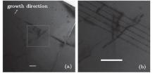
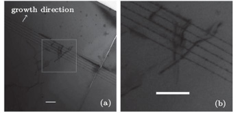
In order to further study the effect of a dot dislocation filter on GaAs/Si epilayers, dislocations in the sample with the dislocation filter of five-layer QDs are observed directly by cross-sectional TEM. Generally, there are two types of threading dislocations in GaAs/Si heteroepitaxy. One is the pure-edge dislocation, and the other is the 60° mixed dislocation. Generally, the former can be annihilated easily by thermal cycle annealing, while the situation of the latter is reversed. Figure 5 shows the interreaction between dislocations and the dislocation filter in a typical region. Figure 5(b) shows an amplified image of the region marked by the white frame in Fig. 5(a). As shown in Fig. 5(a), the dislocations generated from the GaAs/Si interface propagate toward and encounter with the dislocation filter. When dislocations propagate through the dislocation filter, which is shown in Fig. 5(b), they bend and are suppressed, and do not propagate continuously to the upper epilayers anymore.
Fig. 5. Cross-sectional TEM images of dislocation propagation in the five-layer QD dislocation filter, and (b) amplified image of the labeled region in panels (a). The scale bar is 200 nm in both images.
5. Conclusions
In this paper, through experimental study of the multiple QD layers serving as dislocation filters for GaAs/Si epilayers, the growth conditions and the number of dot layers grown by MOCVD are optimized. Using the dot dislocation filters, the dislocation density of the GaAs/Si film reduces up to 2× 106 cm− 2 easily. The results demonstrate that the dislocation density of GaAs/Si epilayers can be reduced by more than one order of magnitude, and multiple dot layers can effectively bend and suppress dislocations in GaAs/Si films for obviously improving the crystalline quantity. Based on our experimental results, proposed is an effective method to further reduce the dislocation density in III– V compound semiconductors grown on silicon, which is the key factor to realizing high-reliability Si-based optoelectronic devices and monolithic integration chips.
... [1,2] Secondly, due to the brittleness and higher cost of GaAs wafers, GaAs/Si epilayers could replace GaAs substrates for applications in high-speed microelectronic[3#cod#x2013 ...
1
2006
0.0
0.0
... [1,2] Secondly, due to the brittleness and higher cost of GaAs wafers, GaAs/Si epilayers could replace GaAs substrates for applications in high-speed microelectronic[3#cod#x2013 ...
1
2012
0.0
0.0
... [1,2] Secondly, due to the brittleness and higher cost of GaAs wafers, GaAs/Si epilayers could replace GaAs substrates for applications in high-speed microelectronic[3#cod#x2013 ...
Metal-insulator-semiconductor back contact has been employed for a perovskite organic lead iodide heterojunction solar cell, in which an ultrathin Al2O3 film as an insulating layer was deposited onto the CH3NH3PbI3 by atomic layer deposition technology. The light-to-electricity conversion efficiency of the devices is significantly enhanced from 3.30% to 5.07%. Further the impedance spectrum reveals that this insulating layer sustains part of the positive bias applied in the absorber region close to the back contact and decreases the carrier transport barrier, thus promoting transportation of carriers.
Effects of an ultra-strong magnetic field on electron capture rates for Co-55 are analyzed in the nuclear shell model and under the Landau energy levels quantized approximation in the ultra-strong magnetic field, and the electron capture rates on 10 abundant iron group nuclei at the surface of a magnetar are given. The results show that electron capture rates on Co-55 are increased greatly in the ultra-strong magnetic field, by about 3 orders of magnitude generally. These conclusions play an important role in future study of the evolution of magnetars.
Du Jun 1 ;Li Ping-Ping 1 ;Luo Xia 1,2 ;
Effects of ultra-strong magnetic field on electron capture rates for 55 Co are analyzed in the nuclear shell model and under the Landau energy levels quantized approximation in the ultra-strong magnetic field, and the electron capture rates on 10 abundant iron group nuclei at the surface of magnetar are given. The results show that electron capture rates on 55 Co are increased greatly in the ultra-strong magnetic field, by about 3 orders of magnitude generally. These conclusions play an important role in future studying the evolution of magnetar.
... 10] Finally, optoelectronic integrated circuits on silicon chips attract ever-increasing attention in the need of high-bandwidth optical interconnects ...
1
2011
27.254
0.0
... [11#cod#x2013 ...
1
2010
27.254
0.0
2
2008
1.865
0.0
... 13] ...
... [13,14] In order to improve the crystalline quality, various defect reduction methods have been proposed in the past two decades, such as the two-step growth, thermal cycle annealing, strained-layer superlattices (SLS), and patterned substrates ...
1
1999
3.794
0.0
... [13,14] In order to improve the crystalline quality, various defect reduction methods have been proposed in the past two decades, such as the two-step growth, thermal cycle annealing, strained-layer superlattices (SLS), and patterned substrates ...
2
2008
0.71
0.0
... [15#cod#x2013 ...
... In our previous investigations, the two-step growth of GaAs/Si epilayers[15#cod#x2013 ...
Metal-insulator-semiconductor back contact has been employed for a perovskite organic lead iodide heterojunction solar cell, in which an ultrathin Al2O3 film as an insulating layer was deposited onto the CH3NH3PbI3 by atomic layer deposition technology. The light-to-electricity conversion efficiency of the devices is significantly enhanced from 3.30% to 5.07%. Further the impedance spectrum reveals that this insulating layer sustains part of the positive bias applied in the absorber region close to the back contact and decreases the carrier transport barrier, thus promoting transportation of carriers.


 , Hu Hai-Yang, Deng Can, He Yun-Rui, Wang Qi, Duan Xiao-Feng, Huang Yong-Qing, Ren Xiao-Min]