Zheng Yan-Qiong, William J. Potscavage, Zhang Jian-Hua, Wei Bin, Huang Rong-Juan. Hole transporting material 5, 10, 15-tribenzyl-5H-diindolo[3, 2-a:3′, 2′-c]-carbazole for efficient optoelectronic applications as an active layer* . Chinese Physics B, 2014, 24(2): 027801
Permissions
Hole transporting material 5, 10, 15-tribenzyl-5H-diindolo[3, 2-a:3′, 2′-c]-carbazole for efficient optoelectronic applications as an active layer*
Zheng Yan-Qionga),b), William J. Potscavageb), Zhang Jian-Huaa)†, Wei Bina), Huang Rong-Juana)
Key Laboratory of Advanced Display and System Applications, Ministry of Education, Shanghai University, Shanghai 200072, China
Center for Organic Photonics and Electronics Research (OPERA) and International Institute for Carbon Neutral Energy Research (WPI-I2CNER), Kyushu University, 744 Motooka, Nishi, Fukuoka 819-0395, Japan
Project supported by the Funding Program for World-Leading Innovative R & D on Science and Technology (FIRST) from JSPS, the Fund from the Science and Technology Commission of Shanghai Municipality, China (Grant Nos. 14DZ2280900 and 14XD1401800), and the Natural Science Foundation of Shanghai (Grant No. 15ZR1416600).
Abstract
In order to explore the novel application of the transparent hole-transporting material 5,10,15-tribenzyl-5H-diindolo[3,2-a:3′,2′-c]-carbazole (TBDI), in this article TBDI is used as an active layer but not a buffer layer in a photodetector (PD), organic light-emitting diode (OLED), and organic photovoltaic cell (OPV) for the first time. Firstly, the absorption and emission spectra of a blend layer comprised of TBDI and electron-transporting material bis-(2-methyl-8-quinolinate) 4-phenylphenolate (BAlq) are investigated. Based on the absorption properties, an organic PD with a peak absorption at 320 nm is fabricated, and a relatively-high detectivity of 2.44 × 1011 cm·Hz1/2/W under 320-nm illumination is obtained. The TBDI/tris (8-hydroxyquinoline) aluminum (Alq3) OLED device exhibits a comparable external quantum efficiency and current efficiency to a traditional 4, 4-bis[N-(1-naphthyl)-N-phenyl-amino]biphenyl ( α-NPD)/Alq3 OLED. A C70-based Schottky junction with 5 wt%-TBDI yields a power conversion efficiency of 5.0%, which is much higher than 1.7% for an α-NPD-based junction in the same configuration. These results suggest that TBDI has some promising properties which are in favor of the hole-transporting in Schottky junctions with a low-concentration donor.
Organic optoelectronic devices have achieved enormous improvements in performance. Basically, several strategies such as synthesis of donors with a suitable energy level or designing novel and efficient device architecture could improve the performance.[1] In addition to the active layers, the improvement in the buffer layer also plays an important role in achieving higher performances of organic optoelectronic devices, such as the novel single buffer layer or the molybdenum oxide/organic mixed buffer layers.[2– 4]
However, the low hole mobility of hole-transporting or extracting material in many cases limit its overall performances. Hole-transporting material possessing a high hole mobility, well-matched ionization potential with the donors, and a high glass transition temperature could address some critical performance issues. The hole-transporting material 5, 10, 15-tribenzyl-5H-diindolo[3, 2-a:3′ , 2′ -c]-carbazole (TBDI) was newly synthesized and just used as an anode buffer layer to improve the performance of subphthalocyanine (SubPc)-based planar heterojunction photovoltaics[5] because of its high hole mobility (5.95 × 10− 3 cm2· V− 1· s− 1) at an electric field of 0.3 MV cm− 1, well-matched highest occupied molecular orbital (HOMO) level, and excellent morphological stability. These properties overcome the deficiencies of low hole mobility for 4, 4′ , 4″ -tri-(2-methylphenyl phenylamino) triphenylaine (m-MTDATA), [6] and of a lack of thermal and morphological stability for 4, 4′ -bis (3-methyl phenylphenylamino) biphenyl (TPD).[7] These advantages imply that TBDI could work well as an anode buffer layer, however, there has been no report about the device performance with TBDI as an active material but not buffer layers to date. Here, we expand the application of TBDI to the active layer for the first time in a photodetector (PD), organic light-emitting diode (OLED), and organic photovoltaic (OPV) cell in this article, a much higher power conversion efficiency (η PCE) from TBDI than from a traditional hole-transporting material in the OPV cell is achieved.
2. Experiment
All the organic materials were purchased commercially from Wako Pure Chemicals Industries, Ltd. (Osaka, Japan) and used after once purification by vacuum gradient sublimation (purity of about 99% ), except for TBDI and C70. TBDI with a purity of > 98% was purchased from Luminescence Technology Corp. (Taiwan) and C70 with a purity of 98% was purchased from Materials Technologies Research, Ltd. (Cleveland, USA), which were used without further purification. Organic and metal layers were sequentially deposited on clean patterned ITO glass substrates with a sheet resistance of 15 Ω /square and an area of 0.04 cm2 through a shadow mask. A poly(3, 4-ethylenedioxythiophene):poly(styrenesulfonate)(PEDOT:PSS, Clevios, PVP AI 4083) layer with a thickness of 20 nm was first spin coated (3000 rpm, 60 s) on the ITO substrate and then annealed for 10 min at 200 ° C in air. The evaporation rates of organic and metal layers were about 0.04 nm/s and 0.3 nm/s, and the evaporation-rate ratio of the TBDI:C70 blend layer was 1:19.
The current density versus voltage (J– V) characteristics of OPV were measured in air without encapsulation, in the dark and under the illumination of an AM1.5 G (1000 W/m2) solar simulator (SRO-25GD, Bunko Keiki Co., Japan). To measure the external quantum efficiency (EQE) spectra, monochromatic light was generated using a Xe arc lamp in conjunction with a monochromator (Bunko Keiki M25-T). During EQE measurements, the wavelength was controlled with a monochromator from 200 nm to 1100 nm. The J– V characteristics of PD were measured in air without encapsulation under the illumination of a monochromated Xe arc lamp (320 nm or 365 nm). The current density– voltage– luminance (J– V– L) characteristics and electroluminescence (EL) spectra of OLED were measured and recorded by a testing setup comprising of a Keithley 2400 source-meter and a Minolta PR-6500 spectrometer. The absorption and photoluminescence (PL) spectra were recorded with a spectrophotometer (LAMBDA950-PKA, PerkinElmer) and a spectrofluorometer (Fluoro Max-4, Horiba Co.). The HOMO levels were measured by ultra-violet photoelectron spectroscopy (AC-2, Riken Keiki Co.).
3. Results and discussion
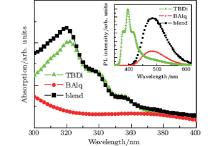
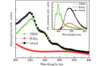
Figure 1 shows the absorption spectra of TBDI, bis-(2-methyl-8-quinolinate) 4-phenylphenolate (BAlq), and a blend film, with the corresponding PL spectra in the inset. In the blend film, the absorption peak is located at 320 nm, near the maximum peak of a pristine TBDI film. The PL peaks of TBDI, BAlq, and the blend films are located at 397, 485, and 485 nm, respectively. The emission of the TBDI:BAlq blend film mainly comes from BAlq. The enhancement of the blend emission together with the disappearance of TBDI emission implies that energy transfer occurs from TBDI to BAlq, [8] which is similar to the energy transfer in a TPD:tris(8-hydroxyquinoline) aluminum (Alq3) system.[9] Most of the research on organic PDs has focused on the ultraviolet (UV) and near infrared wavelength range in recent years, and the relatively-narrow absorption maximum at 320 nm suggests that the TBDI:BAlq blend can be applied to ultraviolet PDs.
Fig. 1. Absorption spectra of 30-nm-thick pristine TBDI and BAlq films as well as 60-nm 1:1 TBDI: BAlq mixed film. The inset shows the corresponding PL spectra.
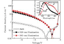
In order to obtain a higher photocurrent response than that of the planar heterojunction PD, a hybrid planar mixed heterojunction (PMHJ) PD with the device configuration of ITO (150 nm)/poly(3, 4-ethylene dioxythiophene):poly (styrenesulfonate) (PEDOT:PSS) (20 nm)/TBDI (15 nm)/ TBDI:BAlq (1:1, 50 nm)/BAlq (20 nm)/LiF (1 nm)/Al (80 nm) is fabricated. The inset of Fig. 2 depicts the photocurrent spectral response and EQE dependence on wavelength at zero bias. The EQE spectrum is located almost entirely in the UV region from 300 nm to 400 nm. Figure 2 illustrates the J– V characteristics under the illumination of 320-nm and 365-nm UV light as well as in the dark. The photocurrent densities are 20.2 μ A/cm2 and 27.8 μ A/cm2 at − 8 V and yield responses of 142 mA/W and 58 mA/W under 320-nm and 365-nm illumination, respectively. The dark current density is 0.94 μ A/cm2 at − 8 V. The response under 365-nm illumination is lower than that (513 mA/W) of an m-MTDATA:BAlq PD[10] because of the radiative energy loss of the TBDI:BAlq blend (inset of Fig. 1), but it is higher than that (30 mA/W) of a TPD:Alq3 PD.[9, 11] We obtain detectivities of 2.44 × 1011 cm· Hz1/2/W and 1.05 × 1011 cm· Hz1/2/W under 320-nm and 365-nm illumination, [12] respectively, which are comparable to squaraine-based near infrared PDs[13] and ITO-free deep ultraviolet PDs.[14]
Fig. 2.J– V characteristics of the hybrid PMHJ PD in the dark and under constant illumination of 320-nm (intensity of 0.142 mW/cm2) and 365-nm (intensity of 0.480 mW/cm2) UV light. The inset shows the photocurrent spectral response and EQE spectrum of the PD at zero bias.
The HOMO level of TBDI is measured to be 5.48 eV by AC-2 in our group, which is deeper than the reported value of 5.25 eV measured by the cyclic voltammetry.[1] Considering a similar HOMO level of TBDI to α -NP (5.50 eV), [15] their hole-transporting properties in OLEDs are compared. The OLEDs each with a configuration of ITO (100 nm)/α -NPD or TBDI (50 nm)/Alq3 (50 nm)/LiF (1 nm)/Al (100 nm) are fabricated, and the EQE dependence on current density, the current efficiency dependence on luminance as well as EL spectra of the two OLEDs are depicted in Fig. 3. TBDI and α -NPD-based OLEDs exhibit similar EL spectra with almost an identical peak wavelength, which is independent of the increasing driving voltage. TBDI OLED shows a highest current efficiency (2.76 cd/A) (inset of Fig. 3), which is comparable to that of the α -NPD OLED and the previously reported values of α -NPD/Alq3 OLEDs.[16, 17] TBDI OLED achieves an almost identical maximum EQE of 0.87% to that (0.83% ) of α -NPD OLED with Commission Internationale d’ Eclairage (CIE) x, y color coordinates of (0.20, 0.34), corresponding to the peak emission at about 520 nm (bluish green light). These results imply that TBDI demonstrates a similar hole-transporting property to α -NPD in the OLED device.
Fig. 3. EL EQE as a function of current density. Insets: EL spectra, as well as current efficiency as a function of luminance of TBDI and α -NPD based OLEDs.
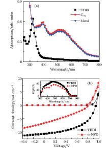
In addition to the deep HOMO energy level, the excellent optical transparency and high hole mobility of TBDI are similar to those of other hole-transporting material 1, 1-bis(4-bis(4-methylphenyl) aminophenyl) cyclohexane (TAPC).[14] Because of the high transparency in the wavelength range of visible light, TBDI was previously just used as a buffer layer in the OPV cell.[5] However, the appropriate HOMO level and high hole mobility of TBDI are suitable for a Schottky junction with a small number of donors, [18] thus we prepare an OPV with a configuration as follows: ITO/PEDOT:PSS (20 nm)/MoO3 (8 nm)/TBDI:C70 (5 wt% , 50 nm)/BCP (10 nm)/Ag (100 nm). An α -NPD-based photovoltaics with the same configuration is also fabricated for comparison. The J– V characteristics as well as EQE spectra are shown in Fig. 4, and photovoltaic characteristics of the two Schottky junctions are summarized in Table 1. It is shown that the η PCE value of the TBDI-based Schottky junction is much higher than that of the α -NPD-based junction and similar to that of a TAPC-based Schottky junction.[19]
Fig. 4. (a) Absorption spectra of 50-nm-thick pristine TBDI and C70 films as well as TBDI:C70 (5 wt% , 50 nm) blend film. (b) J– V characteristics of 5 wt% -donor Schottky junctions with TBDI and α -NPD as donors. Inset shows the EQE spectra.
Table 1.
Table 1.
Table 1. Organic photovoltaic characteristics for ITO/PEDOT:PSS (20 nm)/MoO3 (8 nm)/TBDI or α -NPD:C70 (5 wt% , 50 nm)/BCP (10 nm)/Ag (100 nm), measured in air without encapsulation under illumination of an AM1.5 G solar simulator.
Donor
JSC/mA· cm− 2
VOC/V
FF
η PCE
EQE @475 nm
TBDI
10.64
0.94
0.50
5.0%
72%
α -NPD
6.68
0.81
0.32
1.7%
57%
Table 1. Organic photovoltaic characteristics for ITO/PEDOT:PSS (20 nm)/MoO3 (8 nm)/TBDI or α -NPD:C70 (5 wt% , 50 nm)/BCP (10 nm)/Ag (100 nm), measured in air without encapsulation under illumination of an AM1.5 G solar simulator.
It is estimated that in the 5-wt% -donor blend the electron mobility with about three orders of magnitude higher than that of the hole mobility would be favorable to charge separation.[18] Larger and smaller magnitude differences between donor and electron mobility would reduce the fill factor (FF).[20] In the Schottky junctions including a low-fraction of donors, high μ h in the blend layer is needed to overcome the large hole-hopping distance. Therefore the higher μ h (5.95 × 10− 3 cm2· V− 1· s− 1) in intrinsic TBDI than that (4.80 × 10− 4 cm2· V− 1· s− 1) of α -NPD[21] may contribute to the higher FF, as FF indicates the efficiency of charge transport inside a device and the efficiency of charge collection. The absorption spectra of pristine TBDI and C70 films as well as TBDI:C70 blend film are shown in Fig. 4(a), the light absorption of the blend film with 5-wt% -TBDI mostly originates from the C70 and TBDI contributes little absorption in the wavelength range of visible light. The 5-wt% -TBDI doping efficiently reduces the radiative recombination of the Frenkel excitons in C70, [19] which is responsible for the high short circuit current (JSC). Although TBDI and α -NPD have similar HOMO levels, the TBDI junction demonstrates a higher open circuit voltage (VOC) (0.94 V) than that (0.81 V) for the α -NPD junction, which implies that the VOC not only can be set by the Schottky junction barrier height but also can be strongly influenced by the donor material because of charge trapping, for example.[22] The higher VOC also contributes to the final overall η PCE.
4. Conclusions
We demonstrate the characteristics of TBDI in organic PD, OLED, and OPV devices as an active layer but not just a buffer layer. A TBDI:BAlq combination could be used as a PD with response at 320 nm. TBDI exhibits a comparable EQE and current efficiency to the α -NPD-based OLED, and a much higher η PCE than α -NPD in a 5-wt% -donor Schottky junction. Although TBDI just shows comparable performances in PD and OLED to the conventional hole-transporting material, however, the 5-wt% -TBDI Schottky junction indicates an excellent η PCE of 5.0% . The results imply that the TBDI has some promising properties which are in favor of the hole-transporting in Schottky junctions with low-concentration donor. Further investigation is needed for the detailed properties of TBDI and the working mechanism of harvesting high performance for the TBDI-based Schottky junction.
Acknowledgment
The authors would like to specially thank the Chihaya Adachi Laboratory in Kyushu University (Japan) for preparing a part of the experiments there.
YangQ Q, YangD B, ZhaoS L, HuangY, XuZ, GongW, FanX, LiuZ F, HuangQ Y and XuX R2014Chin. Phys. B23038405DOI:10.1088/1674-1056/23/3/038405[Cited within:1][JCR: 1.148][CJCR: 1.2429]
3
WangN N, YuJ S, ZangY and JiangY D2010Chin. Phys. B19038602DOI:10.1088/1674-1056/19/3/038602[Cited within:1][JCR: 1.148][CJCR: 1.2429]
4
ZhaoL, LiuD Y, LiuD M, ChenP, ZhaoY and LiuS Y2012Acta Phys. Sin. 610088802(in Chinese)DOI:10.7498/aps.61.088802[Cited within:1][JCR: 1.016][CJCR: 1.691]
Effects of an ultra-strong magnetic field on electron capture rates for Co-55 are analyzed in the nuclear shell model and under the Landau energy levels quantized approximation in the ultra-strong magnetic field, and the electron capture rates on 10 abundant iron group nuclei at the surface of a magnetar are given. The results show that electron capture rates on Co-55 are increased greatly in the ultra-strong magnetic field, by about 3 orders of magnitude generally. These conclusions play an important role in future study of the evolution of magnetars.
Du Jun 1 ;Li Ping-Ping 1 ;Luo Xia 1,2 ;
Effects of ultra-strong magnetic field on electron capture rates for 55 Co are analyzed in the nuclear shell model and under the Landau energy levels quantized approximation in the ultra-strong magnetic field, and the electron capture rates on 10 abundant iron group nuclei at the surface of magnetar are given. The results show that electron capture rates on 55 Co are increased greatly in the ultra-strong magnetic field, by about 3 orders of magnitude generally. These conclusions play an important role in future studying the evolution of magnetar.
... [1] In addition to the active layers, the improvement in the buffer layer also plays an important role in achieving higher performances of organic optoelectronic devices, such as the novel single buffer layer or the molybdenum oxide/organic mixed buffer layers ...
... [1] Considering a similar HOMO level of TBDI to #cod#x03B1 ...
1
2014
1.148
1.2429
... [2#cod#x2013 ...
1
2010
1.148
1.2429
1
2012
1.016
1.691
... 4] ...
2
2013
0.0
0.0
... -c]-carbazole (TBDI) was newly synthesized and just used as an anode buffer layer to improve the performance of subphthalocyanine (SubPc)-based planar heterojunction photovoltaics[5] because of its high hole mobility (5 ...
... [5] However, the appropriate HOMO level and high hole mobility of TBDI are suitable for a Schottky junction with a small number of donors,[18] thus we prepare an OPV with a configuration as follows: ITO/PEDOT:PSS (20 nm)/MoO3 (8 nm)/TBDI:C70 (5 wt#cod#x0025 ...
1
2010
3.836
0.0
... -tri-(2-methylphenyl phenylamino) triphenylaine (m-MTDATA),[6] and of a lack of thermal and morphological stability for 4, 4#cod#x02032 ...
1
2001
1.846
0.0
... [7] These advantages imply that TBDI could work well as an anode buffer layer, however, there has been no report about the device performance with TBDI as an active material but not buffer layers to date ...
1
2002
0.71
0.0
... The enhancement of the blend emission together with the disappearance of TBDI emission implies that energy transfer occurs from TBDI to BAlq,[8] which is similar to the energy transfer in a TPD:tris(8-hydroxyquinoline) aluminum (Alq3) system ...
2
2008
3.794
0.0
... [9] Most of the research on organic PDs has focused on the ultraviolet (UV) and near infrared wavelength range in recent years, and the relatively-narrow absorption maximum at 320 nm suggests that the TBDI:BAlq blend can be applied to ultraviolet PDs ...
... [9,11] We obtain detectivities of 2 ...
1
2010
3.794
0.0
... The response under 365-nm illumination is lower than that (513 mA/W) of an m-MTDATA:BAlq PD[10] because of the radiative energy loss of the TBDI:BAlq blend (inset of Fig ...
1
2007
3.794
0.0
... [9,11] We obtain detectivities of 2 ...
1
2009
0.0
0.0
... Hz1/2/W under 320-nm and 365-nm illumination,[12] respectively, which are comparable to squaraine-based near infrared PDs[13] and ITO-free deep ultraviolet PDs ...
1
2011
3.794
0.0
... Hz1/2/W under 320-nm and 365-nm illumination,[12] respectively, which are comparable to squaraine-based near infrared PDs[13] and ITO-free deep ultraviolet PDs ...
2
2011
3.385
0.0
... [14] ...
... [14] Because of the high transparency in the wavelength range of visible light, TBDI was previously just used as a buffer layer in the OPV cell ...
1
2013
3.836
0.0
... 50 eV),[15] their hole-transporting properties in OLEDs are compared ...
We propose a route to examine the thermal degradation of organic light-emitting diodes (OLEDs) with infrared (IR) imaging and impedance spectroscopy. Four different OLEDs with tris (8-hydroxyquinolinato) aluminum are prepared in this study for the analysis of thermal degradation. Our comparison of the thermal and electrical characteristics of these OLEDs reveals that the real-time temperatures of these OLEDs obtained from the IR images clearly correlate with the electrical properties and lifetimes. The OLED with poor electrical properties shows a fairly high temperature during the operation and a considerably short lifetime. Based on the correlation of the real-time temperature and the performance of the OLEDs, the impedance results suggest different thermal degradation mechanisms for each of the OLEDs. The analysis method suggested in this study will be helpful in developing OLEDs with higher efficiency and longer lifetime. (C)2013 Optical Society of America
Kwak, Kiyeol 1 ;Cho, Kyoungah 1 ;Kim, Sangsig 1 ;
... [16,17] TBDI OLED achieves an almost identical maximum EQE of 0 ...
Filamentary discharges in dielectric barrier discharge operating in a glow regime are studied by use of two-dimensional particle-in-cell simulation with Monte Carlo collisions included. The formation of multiple filaments and the involved electric fields, electric potentials, plasma densities, and particle temperatures are presented. It is found that the filaments are not ignited simultaneously, and they expire with the shift of the plasma sheaths. "Dark discharges", which produce ion densities lower by one order of magnitude than a typical filamentary discharge, are observed while the filaments from earlier discharges are decaying. (C) 2013 American Institute of Physics. [http://dx.doi.org/10.1063/1.4794824]
... [16,17] TBDI OLED achieves an almost identical maximum EQE of 0 ...
2
2011
14.829
0.0
... [5] However, the appropriate HOMO level and high hole mobility of TBDI are suitable for a Schottky junction with a small number of donors,[18] thus we prepare an OPV with a configuration as follows: ITO/PEDOT:PSS (20 nm)/MoO3 (8 nm)/TBDI:C70 (5 wt#cod#x0025 ...
... [18] Larger and smaller magnitude differences between donor and electron mobility would reduce the fill factor (FF) ...
Filamentary discharges in dielectric barrier discharge operating in a glow regime are studied by use of two-dimensional particle-in-cell simulation with Monte Carlo collisions included. The formation of multiple filaments and the involved electric fields, electric potentials, plasma densities, and particle temperatures are presented. It is found that the filaments are not ignited simultaneously, and they expire with the shift of the plasma sheaths. "Dark discharges", which produce ion densities lower by one order of magnitude than a typical filamentary discharge, are observed while the filaments from earlier discharges are decaying. (C) 2013 American Institute of Physics. [http://dx.doi.org/10.1063/1.4794824]
... -TBDI doping efficiently reduces the radiative recombination of the Frenkel excitons in C70,[19] which is responsible for the high short circuit current (JSC) ...
1
2011
3.794
0.0
... [20] In the Schottky junctions including a low-fraction of donors, high #cod#x03BC ...
1
2011
2.145
0.0
... -NPD[21] may contribute to the higher FF, as FF indicates the efficiency of charge transport inside a device and the efficiency of charge collection ...
1
2013
3.836
0.0
... [22] The higher VOC also contributes to the final overall #cod#x03B7 ...
Hole transporting material 5, 10, 15-tribenzyl-5H-diindolo[3, 2-a:3′, 2′-c]-carbazole for efficient optoelectronic applications as an active layer*
[Zheng Yan-Qionga),b), William J. Potscavageb), Zhang Jian-Huaa)†, Wei Bina), Huang Rong-Juana)]


 , Wei Bin