Transport mechanism of reverse surface leakage current in AlGaN/GaN high-electron mobility transistor with SiN passivation*
Zheng Xue-Fenga),b)†, Fan Shuanga),b), Chen Yong-Hea),b), Kang Dia),b), Zhang Jian-Kuna),b), Wang Chonga),b), Mo Jiang-Huic), Li Liangc), Ma Xiao-Huab), Zhang Jin-Chenga),b), Hao Yuea),b)
School of Microelectronics, Xidian University, Xi’an 710071, China
Key Laboratory of Wide Bandgap Semiconductor Materials and Devices, Xidian University, Xi’ an710071, China
National Key Laboratory of Application Specific Integrated Circuit (ASIC), Hebei Semiconductor Research Institute, Shijiazhuang 050051, China

Corresponding author. E-mail: xfzheng@mail.xidian.edu.cn

Project supported by the National Natural Science Foundation of China (Grant Nos. 61334002, 61106106, and 61474091), the Opening Project of Science and Technology on Reliability Physics and Application Technology of Electronic Component Laboratory, China (Grant No. ZHD201206), the New Experiment Development Funds for Xidian University, China (Grant No. SY1213), the 111 Project, China (Grant No. B12026), the Scientific Research Foundation for the Returned Overseas Chinese Scholars, State Education Ministry, China, and the Fundamental Research Funds for the Central Universities, China (Grant No. K5051325002).

Abstract

The transport mechanism of reverse surface leakage current in the AlGaN/GaN high-electron mobility transistor (HEMT) becomes one of the most important reliability issues with the downscaling of feature size. In this paper, the research results show that the reverse surface leakage current in AlGaN/GaN HEMT with SiN passivation increases with the enhancement of temperature in the range from 298 K to 423 K. Three possible transport mechanisms are proposed and examined to explain the generation of reverse surface leakage current. By comparing the experimental data with the numerical transport models, it is found that neither Fowler–Nordheim tunneling nor Frenkel–Poole emission can describe the transport of reverse surface leakage current. However, good agreement is found between the experimental data and the two-dimensional variable range hopping (2D-VRH) model. Therefore, it is concluded that the reverse surface leakage current is dominated by the electron hopping through the surface states at the barrier layer. Moreover, the activation energy of surface leakage current is extracted, which is around 0.083 eV. Finally, the SiN passivated HEMT with a high Al composition and a thin AlGaN barrier layer is also studied. It is observed that 2D-VRH still dominates the reverse surface leakage current and the activation energy is around 0.10 eV, which demonstrates that the alteration of the AlGaN barrier layer does not affect the transport mechanism of reverse surface leakage current in this paper.

Keyword: 73.40.Kp; 73.61.Ey; 78.30.Fs; AlGaN/GaN HEMTs; reverse surface leakage current; transport mechanism; 2D-VRH
1. Introduction

Due to the high electron saturation velocity, high breakdown electric field, and good thermal and chemical stability, AlGaN/GaN high-electron mobility transistors (HEMTs) are developed for applications in high-power switches, digital ICs, high-frequency microwave amplifiers, and high-temperature semiconductor devices.[14] One of the critical issues that remains to be studied for GaN HEMTs is the excessive reverse gate leakage current, which increases the low frequency noise, reduces the power added efficiency, causes the current collapse effect, and lowers the breakdown voltage.[5] In general, the overall gate leakage current includes several components, such as surface leakage, bulk leakage, and mesa leakage. To further improve the operation frequency, the characteristic size of the Schottky gate in GaN HEMT needs to be further reduced, then the spacing between the gate and the Ohmic contact will be downscaled accordingly.[6, 7] Consequently, the electric field between the Schottky gate electrode and the Ohmic contact increases rapidly, which will induce significant lateral electron injection from the gate edge to the AlGaN surface and form the reverse surface leakage current. Therefore, the surface leakage current will play an increasingly important role in realizing the GaN HEMTs.

In previous works, most studies focused on the overall reverse gate leakage current by utilizing Schottky diode structures, in which the surface leakage current is only one component.[810] In order to study the transport mechanism of surface leakage current, Tan et al.[11] proposed a dual-gate structure, in which an additional Schottky gate was located between the main Schottky gate and the Ohmic contact, to realize the separation of surface leakage current and bulk leakage current. A Frenkel– Poole emission model has been proposed to explain the transport mechanism of surface leakage current in AlGaN/GaN HEMT without or with low-temperature deposition of SiN, of which the transport mechanism, however, in HEMT with a standard SiN passivation layer is still not clear yet. Based on the above proposed dual-gate structure, Kotani et al.[12] studied the reverse surface leakage current in HEMT with an i-AlGaN/n-AlGaN/i-AlGaN/GaN structure grown by molecular-beam epitaxy. A two-dimensional variable range hopping (2D-VRH) assisted by high-density surface states was proposed to explain the transport mechanism of surface leakage current, based on a device without the SiN passivation layer. However, to date, most of the HEMTs have been passivated by SiN to suppress the current collapse in operation. Liu et al.[13] have investigated the surface leakage current in GaN HEMT on high-resistivity silicon substrate with different passivation layers, and concluded that the passivation material has a great influence on the activation energy. Considering the fact that the devices in previous studies are evidently different in structure, passivation layer, electrode spacing, electrode configuration, etc., a thorough investigation on the transport mechanism is still lacking and pressingly required.

In this paper, the transport mechanism of reverse surface leakage current in AlGaN/GaN HEMT with SiN passivation is studied. By utilizing a dual-gate structure, the reverse surface leakage current can be accurately assessed. The dependence of reverse surface leakage current on temperature is investigated. Three transport mechanisms are proposed to demonstrate the surface leakage current, respectively. Meanwhile, the activation energy of surface leakage current is extracted, and the effect of a barrier layer on the transport mechanism of reverse surface leakage current is evaluated as well.

2. Devices and experiments

All the GaN/AlGaN/GaN heterostructures used in this paper were grown on (0001) sapphire substrates by metal– organic chemical vapor deposition (MOCVD). The structure consists (from bottom to top) of an AlN nuclear layer, a 1.3-μ m-thick unintentionally doped GaN buffer layer, a 1-nm-thick AlN interlayer, and a 20-nm thick-undoped Al0.3Ga0.7N barrier layer. Room temperature Hall measurements show an electron sheet density of 1.0× 10¹³  cm-2. The Ohmic contact was obtained by depositing a Ti/Al/Ni/Au (20  nm/180  nm/55  nm/45  nm) multilayer, followed by the rapid thermal annealing at 850  ° C for 30  s in an N2 ambient. A uniform contact resistance about 0.5  Ω · mm was measured from transmission-line matrix patterns. The device mesa isolation was formed by dry etching using a Cl2/Ar plasma in a reactive ion etching (RIE) system. The surface passivation was carried out by depositing an about 60-nm thick Si3N4 layer through the plasma-enhanced chemical vapor deposition (PECVD). The recessed-gate area was formed by contact lithography. The Ni/Au/Ni contact (45  nm/200  nm/20  nm) deposition and liftoff were performed to form the Schottky gate.

To investigate the reverse surface leakage current, a dual-gate structure[11] is utilized to separate it from the overall gate leakage current. As shown in Fig.  1, an additional Schottky gate, G2, is located between the conventional Schottky gate, G1, and the Ohmic contact. In this paper, the distance between the additional Schottky gate G2 and the main Schottky gate G1 and the distance between G2 and the Ohmic contact are both 2  μ m. The Schottky gate length and width are 0.8  μ m and 1  mm, respectively.

Fig.  1. Schematic illustration of dual-gate structure and the measurement circuit. During measurement, both G2 and Ohmic contact are grounded, and G1 is reversed-biased. The surface leakage current is collected by G2, and the bulk leakage current is collected by Ohmic contact.

During the measurement, both the G2 electrode and the Ohmic contact are connected to the ground, and the G1 electrode is reverse biased by a negative gate voltage by using an Agilent B1500A semiconductor parameter analyzer. The leakage current that flows through G1 includes two parts. One (Ibulk) flows into the Ohmic contact through the barrier layer and 2DEG channel, which can be measured at the Ohmic contact as the bulk leakage. The other one (Isurf), which is caused by the lateral electron injection from G1 to G2, can be measured at G2 as surface leakage. The arrows in Fig.  1 indicate the direction of electron flow. Figure  2 shows the measured reverse surface leakage current and bulk leakage current at room temperature. It is evidently observed that the surface leakage current can be well separated from the bulk leakage current and is significant in the overall reverse gate leakage current.

Fig.  2. Plots of reverse surface leakage current and bulk leakage current versus VG1 at room temperature, which are extracted by utilizing the dual-gate structure in Fig.  1.

3. Results and discussion

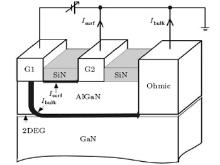
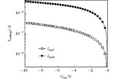
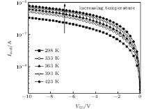
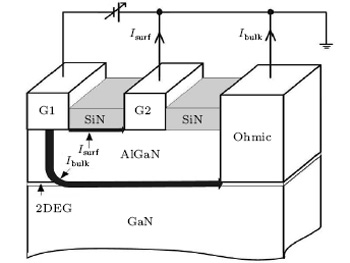
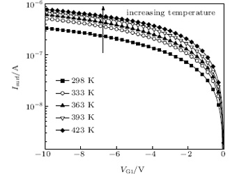
The reverse surface leakage currents at temperatures ranging from 298  K to 423  K are measured by using the dual-gate structure in Fig.  1. As shown in Fig.  3, it is obvious that the surface leakage current has significant dependence on temperature, which is consistent with the result observed in early work.[11, 12] In order to investigate the transport mechanism of surface leakage current, three possible mechanisms are proposed and examined in detail below.

Fig.  3. Variations of reverse surface leakage current with gate bias voltage (VG1) at temperatures ranging from 298  K to 423  K. The device under test is an SiN passivated HEMT with a 20-nm-thick Al0.3Ga0.7N barrier layer.

3.1. Fowler– Nordheim tunneling mechanism

Considering the surface leakage current in AlGaN/GaN HEMT, the mechanism of Fowler– Nordheim (FN) tunneling demonstrates that electrons at the G1 electrode have a possibility to tunnel directly to the G2 electrode under high electric field. The higher electric field will induce a larger FN tunneling current. It accords with the measured results in Fig.  3, in which the surface leakage current increases significantly with the increase of negative gate bias. The FN tunneling model can be numerically expressed as[8]

where J is the current density, both A and B are the constants, and E is the electric field across the barrier layer surface between G1 and G2 in this paper. According to Eq.  (1), the current density in the FN tunneling model depends strongly on the electric field and has little relationship with the temperature. However, figure  3 indicates that the surface leakage current increases rapidly with the enhancement of temperature at a constant gate bias. Therefore, we can conclude that the FN tunneling mechanism has little effect on the transport of reverse surface leakage current in this paper.
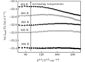
3.2. Frenkel– Poole emission mechanism

In terms of the Frenkel– Poole (FP) emission mechanism, the trapped electrons can get rid of the trap states with the help of the electric field and temperature, and propagate into the threading dislocations related continuum states, [8] which induce the leakage current accordingly. The FP emission model can be expressed as[14]

where T is the temperature; R(T) and S(T) are the slope and intercept of ln(J/E) ∼ E1/2 line, respectively, which can be expressed respectively as[14]

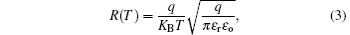
where q is the electron charge, KB is the Boltzmann constant, both π and C are the constants, ɛ r is the relative dielectric constant of AlGaN, ɛ o is the vacuum dielectric permittivity, and ϕ t is the barrier height of the trap energy state with respect to the conductive dislocation state.

Assuming that the FP emission mechanism dominates the transport of surface leakage current, then ln(Jsurf/E) should have a linear dependence on E1/2 according to Eq.  (2). However, this linear relationship is not observed in Fig.  4, which implies that our assumption is incorrect and the FP emission mechanism cannot be used to describe the transport of reverse surface leakage current. Some researchers have claimed that the FP emission mechanism dominates the reverse gate leakage of AlGaN/GaN HEMT in early work.[8, 9, 15] It is worth noting that the surface leakage is only one component of the overall reverse gate leakage. Therefore, it is possible that the transport mechanism of surface leakage current is different from that of the overall reverse gate leakage. It should be noted that the electric field across the surface is complex and not uniformly distributed in general. To simplify this issue, the average electric field is used in this paper.

Fig.  4. Plots of ln(Jsurf/E) versus E1/2 at temperatures ranging from 298  K to 423  K for Schottky gate Al0.3Ga0.7N/GaN HEMT with SiN passivation.

3.3. Two-dimensional variable range hopping (2D-VRH) mechansim

Finally, we examine the third possible mechanism for the transport of surface leakage current under reverse gate bias. The 2D-VRH mechanism, which is assisted by the surface trap states around the AlGaN barrier layer, is proposed to explain this observed phenomenon. According to the 2D-VRH transport model, the conductivity of surface leakage current, σ surf, can be given by[16]

where a is a constant. R is the distance between the initial and final site. Δ E is the energy gap between the initial and final site, which depends on R. In general, there is an optimum combination of R and Δ E, which maximizes the total surface leakage conductivity σ surf. The optimum energy gap Δ E and the distance R for maximum surface conductivity can be determined and shown below, respectively.

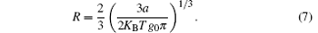
Inserting Eqs.  (6) and (7) into expression  (4) and rearranging terms to separate out the temperature dependence yields the following expression, we have

where T0 is the characteristic temperature. It is obviously observed that the surface leakage conductivity σ surf is strongly dependent on the temperature in the 2D-VRH model.

The activation energy (Ea) of surface leakage current, which reflects the possibility of the 2D-VRH transport process, can also be extracted though a similar expression as shown below[13]

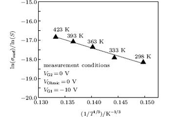
In Fig.  5, plots of ln(σ surf) versus 1/T1/3 at the bias voltage VG1 = − 5  V, − 8  V, and − 10  V are shown, respectively. It is observed that the experimental data for temperatures ranging from 298  K to 423  K can be well fitted by a series of straight lines, which are well consistent with expression  (8) in this work. Therefore, the 2D-VRH transport mechanism can be used to explain the reverse surface leakage current in AlGaN/GaN HEMT with SiN passivation. It is consistent with the observation in HEMT with a Si-doped n-AlGaN barrier layer in previous work.[12] Meanwhile, it should also be noted that the transport mechanism of reverse surface leakage current is independent of the voltage bias across the two electrodes in this paper.

Fig.  5. Plots of ln(σ surf) versus 1/T1/3 at temperatures ranging from 298  K to 423  K at bias voltage VG1 = − 5  V, − 8  V, and − 10  V, respectively.

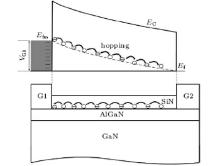
The schematic energy band diagram showing the 2D-VRH transport mechanism of reverse surface leakage current between G1 and G2 is plotted in Fig.  6. As shown in Fig.  6, a number of trap states exist at the AlGaN surface with the energy level close to Fermi level. When a negative bias is applied to G1, the electrons can be injected into the empty surface states from G1 due to the relatively high electric field at the gate edge. Then the injected electrons are possible to be captured by trap states with low potential energy. With the help of the existing electric field and thermal energy, the trapped electrons gain kinetic energy and have a possibility to emit into the trap states with higher potential energy. Considering the potential energy gap existing between those trap states, the electrons that are captured in the higher potential energy traps are unstable, and it is easy for the electrons to fall into the stable state traps with lower potential energy. The electric field applied between the electrodes of G1 and G2 restricts these laterally injected electrons moving from G1 towards G2 via the 2D-VRH model. The movement of these electrons induces the reverse surface leakage current. In other words, the trap states act as “ stepping-stones” for electrons to fall into or emit from them.

Fig.  6. Schematic energy band diagram of the 2D-VRH transport mechanism in dual-gate structure when a negative bias is applied between the electrodes of G1 and G2, which illustrates the electron transport process via surface states between two electrodes, resulting in the lateral surface leakage current in AlGaN/GaN HEMT.

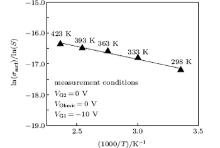
Finally, the Arrhenius curve of ln(σ surf) versus 000/Tis plotted in Fig.  7. Considering expression  (9), the activation energy can be extracted accordingly and is around 0.083  eV, which is different from those in previous studies.[11, 13] It should be noted that either the barrier layer or the passivation layer is obviously different from those in previous studies, which may induce the variation of activation energy. With increasing the temperature, the electrons trapped in surface states gain kinetic energy and have a higher possibility to hop out, which results in the increase of surface leakage current as shown in Fig.  3.

Fig.  7. Plot of ln(σ surf) versus 1000/Tat temperatures ranging from 298  K to 423  K under the bias of VG1 = − 10  V.

In order to further investigate the transport mechanism of reverse surface leakage current, a similar dual-gate structure with different AlGaN barrier layers is adopted. The barrier layer is of 8-nm-thick AlGaN with a high Al composition (65%). A similar temperature-dependent experiment is carried out. Three possible transport mechanisms are examined, separately. It is shown that both the FN tunneling mechanism and FP emission mechanism still cannot be used to explain the generation of surface leakage current. As shown in Fig.  8, only the 2D-VRH model is well consistent with the measured experimental data. Moreover, the activation energy is extracted to be 0.10  eV. It is slightly different from that in HEMT in the case with a conventional AlGaN barrier layer, which may be attributed to the alteration of the barrier layer. Therefore, we can conclude that the 2D-VRH mechanism still dominates the transport of reverse surface leakage current in HEMT with an 8-nm-thick Al0.65Ga0.35N barrier layer, and no new mechanism is introduced in this work. In other words, the alteration of the AlGaN barrier layer has little effect on the transport mechanism of reverse surface leakage current in this paper.

Fig.  8. Plot of ln(σ surf) versus 1/T1/3 at temperatures ranging from 298  K to 423  K under the bias voltage VG1 = − 10  V in SiN passivated HEMT with 8-nm-thick Al0.65Ga0.35N barrier layer.

4. Conclusions

In this paper, the transport mechanism of reverse surface leakage for AlGaN/GaN HEMT with SiN passivation is studied. By utilizing the dual-gate structure, the surface leakage current can be well assessed. Temperature-dependent experiments at temperatures ranging from 298  K to 423  K are carried out. It is observed that the reverse surface leakage current increases with the enhancement of temperature. Associated with the numerical transport models, the mechanisms of Fowler– Nordheim tunneling and Frenkel– Poole emission cannot explain the generation of surface leakage current. However, it is found that the measured experimental data are well accordant with the 2D-VRH model. Therefore, we conclude that the 2D-VRH mechanism dominates the transport of surface leakage current. The activation energy is extracted, which is around 0.083  eV. Furthermore, it is also observed that the 2D-VRH dominates the surface leakage current in SiN passivated HEMT with high Al composition and a thin AlGaN barrier layer. The activation energy is around 0.10  eV. It indicates that the alteration of the AlGaN barrier layer has little influence on the transport mechanism of the surface leakage current in AlGaN/GaN HEMT in this paper.

Reference
1 Cai Y, Cheng Z, Yang Z, Tang C W, Lau K M and Chen K J 2007 IEEE Electron Dev. Lett. 28 328 DOI:10.1109/LED.2007.895391 [Cited within:1]
2 Hu G Z, Yang L, Yuan Y L, Si Q, Gao J S, Gang M J, Hua M X and Yue H 2010 Chin. Phys. Lett. 27 087302 DOI:10.1088/0256-307X/27/8/087302 [Cited within:1] [JCR: 0.811] [CJCR: 0.4541]
3 Del Alamo J A and Joh J 2009 Microelectron. Reliab. 49 1200 DOI:10.1016/j.microrel.2009.07.003 [Cited within:1] [JCR: 1.137]
4 Wang R, Cai Y and Chen K J 2009 Solid-State Electron. 53 1 DOI:10.1016/j.sse.2008.09.001 [Cited within:1] [JCR: 1.482]
5 Marcon D, Viaene J, Favia P, Bender H, Kang X, Lenci S, S S and Decoutere S 2012 Microelectron. Reliab. 52 2188 DOI:10.1016/j.microrel.2012.06.052 [Cited within:1] [JCR: 1.137]
6 Kong X, Wei K, Liu G and Liu X 2012 Chin. Phys. Lett. 29 078502 DOI:10.1088/0256-307X/29/7/078502 [Cited within:1] [JCR: 0.811] [CJCR: 0.4541]
7 Bouzid-Driad S, Maher H, Defrance N, Hoel V, De Jaeger J C, Renvoise M and Frijlink P 2013 IEEE Electron Dev. Lett. 34 36 DOI:10.1109/LED.2012.2224313 [Cited within:1]
8 Zhang H, Miller E J and Yu E T 2006 J. Appl. Phys. 99 023703 DOI:10.1063/1.2159547 [Cited within:4] [JCR: 0.71]
9 Arslan E, Bütün S and Ozbay E 2009 Appl. Phys. Lett. 94 142106 DOI:10.1063/1.3115805 [Cited within:1] [JCR: 3.794]
10 Yan D, Lu H, Cao D, Chen D, Zhang R and Zheng Y 2010 Appl. Phys. Lett. 97 153503 DOI:10.1063/1.3499364 [Cited within:1] [JCR: 3.794]
11 Tan W S, Uren M J, Houston P A, Green R T, Balmer R S and Martin T 2006 IEEE Electron Dev. Lett. 27 1 DOI:10.1109/LED.2005.860383 [Cited within:4]
12 Kotani J, Tajima M, Kasai S and Hashizume T 2007 Appl. Phys. Lett. 91 093501 DOI:10.1063/1.2775834 [Cited within:3] [JCR: 3.794]
13 Liu Z H, Ng G I, Zhou H, Arulkumaran S and Maung Y K T 2011 Appl. Phys. Lett. 98 113506 DOI:10.1063/1.3567927 [Cited within:3] [JCR: 3.794]
14 Lin F, Shen B, Lu L, Xu F, Liu X and Wei K 2014 Chin. Phys. B 23 037303 DOI:10.1088/1674-1056/23/3/037303 [Cited within:2] [JCR: 1.148] [CJCR: 1.2429]
15 Rao P K, Park B, Lee S, Noh Y, Kim M and Oh J 2011 J. Appl. Phys. 110 013716 DOI:10.1063/1.3607245 [Cited within:1] [JCR: 0.71]
16 Mott N F and Davis E A 1979 Electronic Porcesses in Non-Crystalline Materials London Clarendon Press [Cited within:1]