Breakdown mechanisms in AlGaN/GaN high electron mobility transistors with different GaN channel thickness values

Breakdown mechanisms in AlGaN/GaN high electron mobility transistors with different GaN channel thickness values |
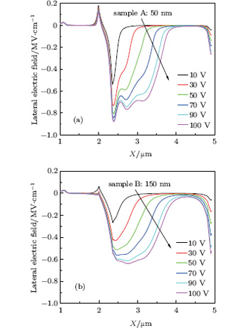
| Lateral electric fields along the channel/ buffer interface of (a) sample A and (b) sample B, with V GS = −6 V applied to the gate and V DS varying from 10 V to 100 V. |
 |