


Breakdown mechanisms in AlGaN/GaN high electron mobility transistors with different GaN channel thickness values*
[Ma Xiao-Huaa) , Zhang Ya-Mana) , Wang Xin-Huab) , Yuan Ting-Tingb) , Pang Leib) , Chen Wei-Weia) , Liu Xin-Yub)†  ]
]
]
|
|


Corresponding author. E-mail: xyliu@ime.ac.cn
Project supported by the Program for New Century Excellent Talents in University (Grant No. NCET-12-0915) and the National Natural Science Foundation of China (Grant Nos. 61334002 and 61204086).
In this paper, the off-state breakdown characteristics of two different AlGaN/GaN high electron mobility transistors (HEMTs), featuring a 50-nm and a 150-nm GaN thick channel layer, respectively, are compared. The HEMT with a thick channel exhibits a little larger pinch-off drain current but significantly enhanced off-state breakdown voltage ( BVoff). Device simulation indicates that thickening the channel increases the drain-induced barrier lowering (DIBL) but reduces the lateral electric field in the channel and buffer underneath the gate. The increase of BVoff in the thick channel device is due to the reduction of the electric field. These results demonstrate that it is necessary to select an appropriate channel thickness to balance DIBL and BVoff in AlGaN/GaN HEMTs.
The GaN-based HEMT is a promising candidate for the next generation of microwave power transistor technology due to its impressive properties, such as high electron saturation velocity, and the high two-dimensional electron gas (2DEG) density at the AlGaN/GaN hetero-interface. AlGaN/GaN HEMT achieves a high power density by means of a large critical breakdown field (∼ 3 MV/cm) and the ability to sustain a large channel current.[1– 3] Breakdown voltage restricts the device maximum output power, device reliability, and consequently the application of GaN-based HEMT.[4] Although many methods to increase the device breakdown voltage, thus improving the device power performance, have been proposed, the detailed breakdown mechanisms in these devices are not exactly known. It is generally believed that several mechanisms may induce breakdown in HEMTs, including excessive gate leakage current, punch through in the buffer underneath the gate, and the presence of an ionization effect in the channel.[3, 5– 9] These effects could be significantly influenced by the localized high electric fields, [10] especially in the channel and buffer at the drain-side edge of the gate, [7] as well as the bulk traps in the buffer layer.[6] The high electric fields and bulk trap can be alleviated by proper field plate and epitaxial engineering, [10] respectively. In most cases, [8] low-Al-composition AlGaN buffer technology, doping compensation, and deep level dopants such as carbon and iron are advantageous to improve the off-state breakdown voltage.[5, 11– 14] Unfortunately, these deep level dopants may aggravate the device current collapse.[15] Therefore, the optimization of epitaxial layers is required to minimize the current collapse and at the same time to enhance values of BVoff of AlGaN/GaN HEMTs. In this work, GaN channel thickness values in AlGaN/GaN HEMTs each with a composite AlGaN/GaN buffer layer are varied to achieve the above goals. Our experiment in Ref. [16] has confirmed that increasing the thickness of the unintentional doped GaN channel can effectively suppress the current collapse. In this paper, off-state breakdown mechanisms in AlGaN/GaN high electron mobility transistors with different GaN channel thickness values are investigated intensively.
Two 2-inch (1 inch = 2.54 cm) AlGaN/GaN HEMT wafers, named samples A and B, were prepared by metal– organic chemical vapor deposition (MOCVD) on SiC substrates. For comparison, the two wafers feature the same epitaxial structure except for the GaN channel layer thickness. The unintentional doped GaN channel layer thickness values for samples A and B were 50 nm and 150 nm, respectively. Their cross-sectional schematic and material parameters are shown in Fig. 1 and Table 1. It is worth noting that a composite AlGaN/GaN buffer, consisting of a 1-μ m-thick Al0.04Ga0.96N and a 1-μ m-thick GaN, was adopted to realize a better 2DEG confinement.[5, 13] The sheet densities of 2DEG for sample A and sample B were 7.2× 1012 cm− 2 and 7.9× 1012 cm− 2, respectively.
 | Fig. 1. Cross-sectional schematic diagram of AlGaN/GaN HEMTs (samples A and B) used in this work. |
| Table 1. Epitaxial structures of compared samples, d denotes thickness, and x the Al concentration. |
Transistor fabrication began with Ohmic contacts formed by an alloyed Ti/Al/Ni/Au metal stack, followed by a 120-nm-thick SiNx surface passivation layer grown at 300 ° C by PECVD. Device isolation was achieved by multiple energy N+ implantations. The 0.35-μ m gate was accomplished by electron beam lithography, dry etching through the PECVD-SiNx layer, and slightly recessing of the GaN cap layer, followed by a second lithography and Schottky gate fabrication formed with Ni and Au. After that, a second PECVD-SiNx of 200 nm was grown to facilitate the fabrication of source-connected field plates.
As shown in Fig. 1, the source– drain distance (LSD) and source– gate spacing (LSG) of both samples are 4 μ m and 1 μ m, respectively. The lengths of the gate-connected field-plate (LGFP) and source-connected field-plate (LSFP) are 0.3 μ m and 0.8 μ m, respectively. The device with a gate width of 1× 100 μ m was tested to achieve direct-current current– voltage (DC I– V) characterization, using an Agilent 4142 device analyzer. The breakdown mechanism is investigated by an Atlas 2D device simulator.
Figure 2 shows the typical transfer characteristics of HEMTs with different GaN channel thickness values used in this work. The trans-conductance peak of sample A is higher than that of sample B, while the threshold voltage (VTH) of sample B is more negative and the saturated output current is larger as illustrated in Fig. 2. This is because sample B presents a wider current path and higher 2DEG concentration.
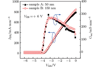 | Fig. 2. Typical transfer characteristics of HEMTs with different channel thickness values (sample A and sample B). |
The value of BVoff is estimated by measuring Ioff– VDS characteristics under the off-state condition (VGS = − 6 V) as shown in Fig. 3. In order to investigate the breakdown mechanism, besides monitoring ID, gate reverse leakage current (IG) and source leakage current (IS) are also measured under the off-state condition. The BVoff is defined as the VDS at which IDoff of 1 mA/mm is reached. In this case, BVoff of sample A is estimated to be 90 V, while that of sample B is much larger than 100 V. IS of sample B is higher than that of sample A. We predict that the larger source leakage current of sample B in region I results from the significant DIBL effect in the buffer layer.
 | Fig. 3. Off-state breakdown characteristics measured at VGS = − 6 V (below VTH) of sample A (a) and sample B (b). The BVoff is defined as the VDS at which ID of 1 mA/mm is reached. |
For both samples, in region I (VDS< 80 V), off-state drain current is dominated by IG. However, the source leakage current starts to increase steeply at VDS = 80 V, causing a rapid rise of pinch-off drain current and leading to device breakdown in sample A as shown in Fig. 3. However, in sample B, neither device breakdown nor the rapid rise in IS can be observed till VDS reaches 100 V. A probable explanation for the breakdown caused by the sudden increase of IS in sample A is that the lateral electric field intensity between the source and drain is higher in sample A.[16]
To the best of our knowledge, the reduction in thickness of the unintentional doped (UID) GaN channel is beneficial for reducing buffer leakage and improving BVoff in a power electronic device.[2, 7, 17] Generally, the breakdown criterion for power electronics is that pinch-off drain current reaches 1 μ A/mm, which is stricter than that of microwave power amplifier (PA) application (1 mA/mm). This is because the operation voltage for a power electronic device is extremely high, and a larger pinch-off current will produce more static power consumption, leading to premature thermal breakdown.[8] Conversely, for microwave PA application in our case, when breakdown criterion is chosen to be 1 mA/mm, BVoff is enhanced in the PA device with the thick GaN channel. In fact, if we choose 1 μ A/mm as the breakdown criterion here, BVoff of sample B would be lower than that of sample A, which is consistent with the case in power electronic devices. But such a strict criterion is unnecessary for a microwave PA device. Since its operation voltage is much lower, and the microwave PA device can withstand the thermal stress caused by the larger pinch-off current, which is acceptable. Therefore, the premature thermal breakdown does not occur in the microwave PA device.
To clarify the source leakage current behaviors in both structures, the energy band and electric field are simulated by an Atlas 2D device simulator. Conduction band energy diagrams of the two samples along the vertical cut-lines passing through the center of the gate with no bias applied and along the horizontal cut-lines in the buffer interface with VGS = − 6 V are plotted in Figs. 4(a) and 4(b), respectively. As shown in Fig. 4(a), the raised conduction band of the channel of sample A enables a good 2DEG confinement, because the electron channel becomes a deep potential well.[5] When no voltage is applied to the device, the barrier height at the channel/buffer interface for sample B is a little higher than that of sample A according to Fig. 4(a). However, it is lower in sample B when a pinch-off bias is applied to the gate as shown in Fig. 4(b). This is due to the gate control becoming worse as the channel becomes thicker.
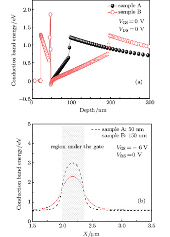 | Fig. 4. Conduction band energy diagrams of devices with different channel thickness values (50 nm and 150 nm) (a) along the vertical cut-lines passing through the center of the gate and down through the buffer at VDS = 0 V and VGS = 0 V, and (b) along the horizontal cut-lines in the channel/ buffer interface, at VDS = 0 V and VGS = − 6 V. |
To show the DIBL more explicitly, figures 5(a) and 5(b) show the simulated barrier height distributions presented by the conduction band energy along the channel/ buffer interface line for the two samples at different drain voltages. The profiles are calculated at a gate bias of − 6 V with drain– source voltages set to be 1 V, 10 V, and 50 V, respectively. As shown in Fig. 5, the energy barrier in the back of the channel becomes increasingly low as the drain– source voltage increases, owing to the electric field induced by the drain– source voltage, commonly called the DIBL effect, which commonly appears in a short channel device, and it occurs after the application of off-state stress.[18, 19] For a device with a shorter channel length, the voltage across the drain and source (VDS) is increased, more field lines penetrate into the inside of the channel from the drain end.[18] Due to the electric field penetration, the barrier height around the channel is lowered, [18, 19] finally allowing electrons from the source region to punch through the buffer layer over the reduced barrier, resulting in buffer leakage currents in both devices. By comparing Fig. 5(a) with Fig. 5(b), it can be seen that the barrier height in the back of the channel of sample B is lower at the same bias state and its DIBL is more serious due to the gate control being worse. DIBL is 1.286 eV for sample A and it is 1.803 eV for sample B, when VDS varies from 1 V to 50 V.
 | Fig. 5. Cross-sectional distributions of conduction band edge energy along the channel/buffer interface when a pinch-off voltage of − 6 V is applied to the gate with values of VDS = 1 V, 10 V, and 50 V for (a) sample A and (b) sample B. The insets show the entire energy barriers. The barrier height decreases as the drain voltage increases. DIBL of sample B is more significant. |
The sub-threshold current density, which contributes to punch-through leakage, increases exponentially as

where

with Δ ϕ b being the barrier height reduction.[21] It can be concluded from Figs. (1a)and (1b) that the higher the barrier reduction, the higher the punch-through leakage is. DIBL for sample B is higher, therefore Δ ϕ b for sample B is higher, thus, leading to higher punch-through leakage than for sample A.
Moreover, the 2DEG channel under the gate is depleted by the gate-induced field in a pinch-off state. But the electrons from the source region bypass this field and travel through the buffer layer into the low barrier region. Due to the serious DIBL under the gate and poor 2DEG confinement caused by the thicker channel, increased electrons are injected from the source to the drain over the reduced barrier, leading to more pronounced source leakage in sample B, when VDS is below 80 V (region I) as shown in Fig. 3.
The breakdown mechanism caused by the pinch-off source leakage current in sample A is explained by the following consideration. The electric fields are calculated at different drain voltages under the off-state condition with VGS = − 6 V, using a simulation. Figure 6 gives the lateral field intensity along the buffer interfaces of sample A and sample B, the field intensities are calculated at VGS = − 6 V and VDS = 50 V respectively. It can be seen that the high electric field peaks resulting from the potential difference are introduced near the edge of the gate.[2] Figure 6 indicates that the lateral electric field in the buffer layer under the gate of sample A is greatly enhanced in comparison with that of sample B at VDS = 50 V. Peak field at the drain side under the gate of sample A is 0.3 MV/cm higher than that of sample B, which means that the electric field peak intensity of sample A is 0.6 times higher than that of sample B, while it is 0.1 MV/cm higher at the source side edge, at VDS = 50 V.
 | Fig. 6. Comparison of lateral field distribution along the channel/ buffer interface for HEMTs with different channel thickness values (50 nm and 150 nm), calculated at VDS = 50 V in off state (VGS = − 6 V), between samples A and B. |
Figure 7 presents the variations of peak lateral electric field along the buffer interface under the gate with drain– source voltage in the range from 10 V to 100 V. The peak field at the drain side edge under the gate increases with the drain voltage increasing in both devices, while the peak at the source edge decreases slightly. For a more detailed presentation of how the lateral electric field changes, figures 8(a) and 8(b)show the lateral electric field profiles at the channel buffer interface under the gate with the applied drain voltage increasing from 10 V to 100 V for samples A and B, respectively. Obviously, figures 8(a) and 8(b) further demonstrate that the high electric fields extend laterally toward the drain contact and the high electric field regions become wider as VDS increases. As shown in Fig. 7, the peak field at the drain side of the gate continues to increase with the drain voltage. In fact, the peak field of sample A is much stronger in the same bias state.
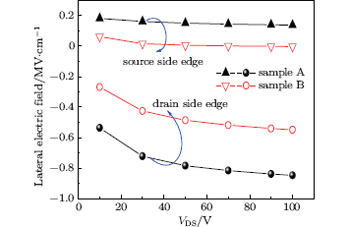 | Fig. 7. Dependences of the peak value of lateral electric field at the buffer interface under the gate on drain– source voltage for sample A and sample B. |
A high electric field in the buffer layer under the gate exceeding a certain threshold creates defects in the vicinity of the high electric field region.[22] Grain-boundary states will be generated due to the high electric field[19] in the channel and buffer layers under the gate. This is because in a region with a high electric field, electrons which obtain enough energy from the high field will impact the lattices. When the energies of electrons exceed a critical value, the electrons cause damage to the lattice and generate defects within the high field region, which is in the drain-access region close to the gate edge.[23] As the lateral electric field in the channel and buffer under the gate increases, the defects will increasingly be produced. The electric field peak will move to higher X and increase with the drain-source voltage as shown in Fig. 8. Correspondingly, the trap generation region will tend to extend laterally toward the drain contact.[23] A high defect density is likely to cause defects to overlap or become larger defect clusters, and then developing into an additional electron leakage path, [24] therefore, triggering the device breakdown. As discussed previously, the simulation results suggest that the lateral electric field under the gate in the channel and buffer layers for the device with a 50-nm-thick channel is much higher, therefore leading to breakdown more easily compared with the device with a 150-nm-thick channel.
 | Fig. 8. Lateral electric fields along the channel/ buffer interface of (a) sample A and (b) sample B, with VGS = − 6 V applied to the gate and VDS varying from 10 V to 100 V. |
In the present work, off-state breakdown voltages and leakage behaviors of HEMTs with different channel thickness values are compared. The experimental results clearly indicate that a thick channel device has a little larger source leakage current but a significantly improved BVoff. Premature breakdown in the thinner channel device is triggered by the sudden rise of source leakage. To investigate the mechanisms, our experimental results are additionally supported by the simulations of energy band and electric field profiles. The simulation evidences that greater source leakage current is caused by the more significant DIBL, and the improved BVoff results from the greatly reduced lateral electric field under the gate in the channel and buffer layer in the thick-channel device. In fact, the thick channel is beneficial for improving power performance at the expense of reducing the frequency features. AlGaN/GaN HEMT therefore requires an optimum thickness of the GaN channel and a proper epitaxial structure to suppress buffer leakage and improve BVoff
| 1 |
|
| 2 |
|
| 3 |
|
| 4 |
|
| 5 |
|
| 6 |
|
| 7 |
|
| 8 |
|
| 9 |
|
| 10 |
|
| 11 |
|
| 12 |
|
| 13 |
|
| 14 |
|
| 15 |
|
| 16 |
|
| 17 |
|
| 18 |
|
| 19 |
|
| 20 |
|
| 21 |
|
| 22 |
|
| 23 |
|
| 24 |
|