Effect of the thickness of InGaN interlayer on a-plane GaN epilayer

Effect of the thickness of InGaN interlayer on a-plane GaN epilayer |
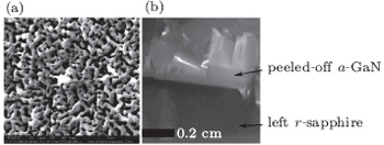
| (a) SEM morphologies of template for sample G and (b) photograph of the peeled-off sample G when cooled down after growth. |
 |