Wang Jian-Xia, Wang Lian-Shan, Zhang Qian, Meng Xiang-Yue, Yang Shao-Yan, Zhao Gui-Juan, Li Hui-Jie, Wei Hong-Yuan, Wang Zhan-Guo. Effect of the thickness of InGaN interlayer on a-plane GaN epilayer* . Chinese Physics B, 2014, 24(2): 026802
Permissions
Effect of the thickness of InGaN interlayer on a-plane GaN epilayer*
Wang Jian-Xiaa),b)†, Wang Lian-Shana)‡, Zhang Qianb), Meng Xiang-Yueb), Yang Shao-Yana), Zhao Gui-Juana), Li Hui-Jiea), Wei Hong-Yuana), Wang Zhan-Guoa)
Key Laboratory of Semiconductor Materials Science, Institute of Semiconductors, Chinese Academy of Sciences, Beijing 100083, China
Patent Examination Cooperation Center of the Patent Office, SIPO, Henan, Zhengzhou 450000, China
Project supported by the National Natural Science Foundation of China (Grant Nos. 91233111, 61274041, and 11275228), the Special Funds for Major State Basic Research Project of China (Grant No. 2012CB619305), the National High Technology R & D Program of China (Grant Nos. 2014AA032603 and 2014AA032609), and the Guangdong Provincial Special Fund for LED Industrial Development, China (Grant No. 2012A080302003).
Abstract
In this paper, we use the a-plane InGaN interlayer to improve the property of a-plane GaN. Based on the a-InGaN interlayer, a template exhibits that a regular, porous structure, which acts as a compliant effect, can be obtained to release the strain caused by the lattice and thermal mismatch between a-GaN and r-sapphire. We find that the thickness of InGaN has a great influence on the growth of a-GaN. The surface morphology and crystalline quality both are first improved and then deteriorated with increasing the thickness of the InGaN interlayer. When the InGaN thickness exceeds a critical point, the a-GaN epilayer peels off in the process of cooling down to room temperature. This is an attractive way of lifting off a-GaN films from the sapphire substrate.
In the past few decades, GaN-based [0001] oriented optoelectronic devices have achieved tremendous progress. However, the device properties are strongly restricted by the existence of the built-in electric fields along the typical [0001] growth direction, caused by the spontaneous and piezoelectric polarizations in the wurtzite nitride materials, leading to the spatial separation of electrons and holes and the decrease of the efficiency.[1] In order to solve the problems, nonpolar a-plane GaN (a-GaN) and m-plane GaN were chosen to make the polarization fields direct to the active quantum-well region of the device. Proof-of-principle experiments have already shown that the devices can have high efficiencies when expensive, small-area bulk non-polar GaN substrates are used.[2] However, for commercially viable devices, costs must be reduced via growing on cheaper and larger substrates such as sapphire or silicon. Unfortunately, in the heteroepitaxy of nonpolar a-GaN, the poor surface morphology always exists, i.e., with triangular/pentagonal pits occurring on the surface[3, 4] and high-density structural defects, including threading dislocations and basal-plane stacking faults (BSFs) bounded by partial dislocations.[5– 8] The quality of the a-GaN film as well as device performance is greatly affected by the pit-surface morphology and the structure defects. Even though the surface pits could be suppressed by growing a-GaN under low V/III ratio and low reactor pressure circumstances, there remain many pronounced striations along the c axis, as many research groups have reported.[9– 13] In the present work, a crucial a-InGaN interlayer is used to fabricate the porous a-GaN template to solve those problems. Our previous results have theoretically proved that the structure of the InGaN interlayer is readily decomposed when the temperature ramps down to 1100 ° C; and then it acts as a weakly bonded layer, which plays a compliant role in improving the crystalline quality and relieving the strain.[14– 16] We also find that the thickness of the InGaN interlayer exerts great influences on the surface morphology, crystalline quality, optical property, and film state, which are thoroughly discussed here in this paper.
2. Experiments
All of the a-GaN samples were grown on r-plane sapphire in a home-made horizontal metal– organic chemical vapor deposition (MOCVD) system by using trimethylgallium (TMGa), trimethylindium (TMI), and ammonia as the precursors. Prior to the epitaxial growth, the r-plane sapphire substrates were annealed at 1100 ° C for 20 min with N2 assistance and nitridized in NH3 atmosphere for 3 min at a flow rate of 3 SLM (where SLM stands for standard liter per minute). Then, different thickness values of InGaN were deposited on the r-plane sapphire substrates at 750 ° C and a pressure of about 2.7× 10⁴ Pa; the flow rates of the TMGa, TMI, and ammonia were 10 μ mol/min, 20 μ mol/min, and 3 SLM, respectively; the percentage of In was approximately 41%. After that, a conventional LT-GaN layer with a thickness of 30 nm was prepared, while the flow rates of the TMGa and ammonia were 35.7 μ mol/min and 3 SLM respectively. Subsequently, a porous GaN template used to release the strain was obtained after annealing the LT-GaN/InGaN/sapphire structures in situ at 1100 ° C for 3 min. Finally, a high-temperature GaN re-growth was performed on the porous GaN template at 1100 ° C and about 6.7× 10³ Pa, the flow rates of TMGa and ammonia were about 35.7 μ mol/min and 0.8 SLM respectively, and the V/III ratio was about 1000, the mixture of N2 and H2 was used as the carrier gas and their ratio was 1:1, i.e., N2:H2= 1:1. The growth parameters of the samples were all the same except the thickness of the InGaN interlayer. The thickness values of InGaN interlayers were determined by SEM to be 0 nm, 76 nm, 114 nm, 171 nm, 205 nm, 240 nm, 258 nm for samples A, B, C, D, E, F, G respectively. The thickness values of the InGaN interlayer and the epilayer state for all the samples are shown in Table 1. For sample G, whose thickness of the InGaN interlayer was 258 nm, the a-GaN epilayer peeled off after it had grown and cooled down to the room temperature, and the peeled-off film was too thin (approximately ∼ 1 μ m) to be unable to be characterized, so the measurements of sample G were removed.
Table 1.
Table 1.
Table 1. Thickness values of the InGaN interlayer and the film states of the samples.
Sample No.
InGaN thickness/nm
Epilayer state
A
0
film
B
76
film
C
114
film
D
171
Film
E
205
film
F
240
part detached
G
258
peel off
Table 1. Thickness values of the InGaN interlayer and the film states of the samples.
The surface morphologies of the samples were investigated by FEI scanning electron microscopy (SEM). The structural properties of the samples were investigated by high-resolution x-ray diffraction (HRXRD) using a Huber five-circle diffractometer at the Diffuse x-ray Scattering Station of the Beijing Synchrotron Radiation Facility. The radiation energy of the light was 8.05 keV, the spot size was 0.7 mm × 0.4 mm (H × V) and the used wavelength was 1.5464 Å .
3. Results and discussion
In Fig. 1, (A1– F1) show the surface morphologies of samples A– F, and (A2– F2) show the cross views of the corresponding samples respectively. Apparently, samples C and D exhibit smooth morphologies without any pit or striation, while samples B and E display smooth morphologies with some pits. Samples A and F present more pits, and some apparent fluctuations orienting to the [0001] direction which is attributed to the fact that the growth rate in the c-axis direction is faster than in the m-axis direction. An appropriate thickness of the InGaN interlayer can effectively improve the surface morphology, and the optimal InGaN thickness for surface morphology is between 114 nm– 171 nm.
As shown in Fig. 1 (A2), sample A has no void in the cross section which implies that the bonding between substrate and epilayer is compact. With an insertion of the InGaN interlayer, the interfaces between r-sapphire substrate and a-GaN epilayer of Samples B and C show some small voids which are produced by the evaporation of In atoms during the in situ high temperature annealing. As the thickness of the InGaN interlayer increases to ∼ 171 nm, the voids of sample D become large. As the thickness of the InGaN interlayer increases up to 205 nm, the voids begin to coalesce. When the thickness increases up to 240 nm, the voids of sample F almost link together and form a long uniform flaw.
Fig. 1. SEM images of a-GaN epilayer of samples A– F.
Many reports showed that the surface pits of a-GaN can be suppressed by preparing samples under a low pressure and low V/III condition, but the striations cannot be eliminated easily. In our work, however, with an appropriate thickness of the a-InGaN interlayer, smooth a-GaN epilayers without any striation can be obtained.
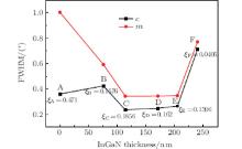
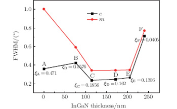
Aiming to obtain the information about the crystal quality of the samples, HRXRD analysis of the ()ω scans as a function of the azimuth angle is performed. The azimuth angles are defined with respect to the [0001] direction. At azimuth 0° , the projection of the incident beam is parallel to the GaN [0001] direction. The InGaN-interlayer-thickness dependences of the full width at half maximum (FWHM) of the () rocking curves for the ∼ 1-μ m-thick a-GaN samples are shown in Fig. 2. The FWHMs of the samples exhibit minimal values when the GaN [0001] direction is in the diffraction plane, and reach their maximal values when the GaN [0001] direction is perpendicular to the diffraction plane. Such a type of in-plane FWHM dependence is consistent with the results reported by others.[17– 19] The FWHMs along c [0001] and directions are given in Fig. 2. As the thickness of the InGaN interlayer increases, the FWHM for the on-axis () XRCs first decreases and then increases. The FWHMs of samples C, D have little difference and the preferable InGaN thickness for a-GaN crystalline quality is between 114 nm– 171 nm. The in-plane crystallographic anisotropy of the a-GaN film can be indicated by the degree of anisotropy ξ , which can be expressed as
The calculated values of the degree of anisotropy ξ for the samples are also shown in Fig. 2. With an insertion of the InGaN interlayer, the values of the degree of anisotropy ξ for samples B, C, D, E, F decrease largely compared with sample A. The degree of anisotropy ξ decreases monotonically with increasing the thickness of the InGaN interlayer. A thick InGaN interlayer is in favor of reducing the anisotropy.
Fig. 2. Dependences of FWHM of the () rocking curves and anisotropy on the thickness of the InGaN interlayer.
The dependence of the degree of anisotropy on the thickness of the InGaN interlayer can be explained by the annealed LT-GaN/InGaN/sapphire templates. The SEM images of the annealed templates are shown in Fig. 3, in which the direction of the arrow represents the [0001] orientation of the a-GaN stripe. Template A without the InGaN interlayer shows a three-dimensional (3D) island morphology, with a size of several micrometers. Template B exhibits stripes along the [0001] direction. Templates (c) and (d) also present porous stripe-like morphologies, but their stripes are more regular and the structures are looser than those sample B presents. The loose and porous stripe structure can act as a compliant template to elastically accommodate lattice mismatch and relieve the strain, thereby improving the growth anisotropy and crystalline quality of a-GaN. As the thickness of the InGaN interlayer increases, the templates (e) and (f) present less anisotropic and eliminate part of the anisotropy. So, the thicker the InGaN interlayer, the looser stripes can be obtained, and the greater the improvement in the surface morphology and the crystal quality will be. The insertion of the InGaN interlayer is a simple, effective way to improve the surface morphology and crystalline quality.
Fig. 3. SEM images of the annealed LT-GaN/InGaN/sapphire templates for samples A– F [corresponding to panels (a)– (f)]. The direction of the arrow represents the [0001] orientation ofa-GaN.
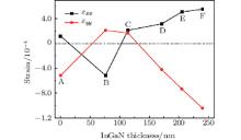
The strains along [] and [] orientations versus InGaN thickness are shown in Fig. 4. Without an InGaN interlayer, the strains of Sample A are tensile and compressive along the x and y directions respectively; with an InGaN interlayer, the strains of samples C, D, E, F are approximately tensile and compressive along the x and y directions respectively. An InGaN interlayer can make the strains ε xx, ε yy change from tensile stress to compressive stress or from compressive stress to tensile stress. It can be concluded that the InGaN interlayer can accommodate the lattice mismatch and thermal mismatch between the a-GaN and the sapphire. For samples B– F, the lattice parameters change monotonically. As the InGaN interlayer increases, the lattice parameters increase along the x direction, and decrease along the y direction. The tendency leads to a region with low strains ε xx and ε yy. When the thickness of the InGaN interlayer is between 101 nm and 130 nm, the strains along the two directions are in a small region.
Fig. 4. Strains of the a-GaN epilayer along [] and [] orientations versus InGaN thickness.
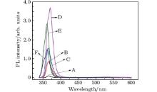
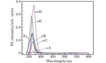
Figure 5 shows the room temperature photoluminescence (PL) spectra of the six a-GaN samples and also the strong band-edge emissions. The yellow luminescence is not apparent compared with the band-emission, which implies the good crystalline quality of the samples. Sample A without the InGaN interlayer shows the weakest intensity. Also, the variation of the intensity with the InGaN interlayer is non-monotonic. For sample D, the PL intensity first increases up to its maximum value, and then decreases with increasing the thickness of the InGaN interlayer. The increase of emission intensity indicates good characteristics of luminescence of the a-GaN sample. In addition to the weaker intensity, the FWHMs of samples E and F also become wider. The PL spectrum density is used to determine the dependence of characteristic luminescence on the thickness of the InGaN interlayer. The fine structure of the PL spectrum may result from the stress in the epilayer, caused by thermal and lattice mismatch, low-dimensional structures formed during growth which leads to a blue shift, and the calibration of the monochromator wavelength. A further low-temperature PL experiment on the fine structure needs to be conducted.
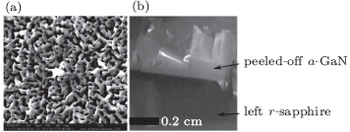
Figure 6 shows the SEM morphologies of the template and the peeled-off a-GaN film for sample G. It can be seen that the morphology of the template presents a porous structure, and the anisotropy also decreases. Figure 6(b) shows the photograph of the peeled-off a-GaN film from the r-sapphire substrate. The strain energy caused by thermal mismatch can be released on the weak bonding layer in the process of cooling. Since the weak bonding layer cannot store the strain energy, the weak bonding layer will break, making the a-GaN epilayer peel off from the substrate. We can hereby control the bonding strength between the film and substrate through controlling the thickness of the InGaN interlayer. If the porous GaN template is used in a MOCVD-HVPE compound device, nonpolar a-GaN thick film can be obtained.
Fig. 6. (a) SEM morphologies of template for sample G and (b) photograph of the peeled-off sample G when cooled down after growth.
4. Conclusions
In this paper, the effect of different thicknesses of InGaN interlayer on a-plane GaN film grown on an r-plane sapphire substrate is discussed. With the InGaN interlayer serving as a compliant layer, pit-free and striation-free a-GaN films are obtained. The surface morphology, crystal quality, and optical properties are all first improved and then deteriorated with increasing the thickness of the InGaN interlayer. If the thickness of the InGaN interlayer increases up to a critical point, the a-GaN film will peel-off.
We would like to express our appreciation to Prof. Wang Huan-Hua and Prof. Jia Quan-Jie (Beijing Synchrotron Radiation Facility, Institute of High Energy Physics, Chinese Academy of Sciences) for their help in HRXRD measurements.
SchmidtM C, KimK C, FarrellR M, FeezellD F, CohenD A, SaitoM, FujitoK, SpeckJ S, DenbaarsS P and NakamuraS2007Jpn. J. Appl. Phys. Part 246L190[Cited within:1][JCR: 1.067]
3
SunQ, YerinoC D, KoT S, ChoY S, LeeIH, HanJ and ColtrinM E2008J. Appl. Phys. 104093523DOI:10.1063/1.3009969[Cited within:1][JCR: 0.71]
4
Holland erJ L, KappersM J, McAleeseC and HumphreysC J2008Appl. Phys. Lett. 92101104DOI:10.1063/1.2830023[Cited within:1][JCR: 3.794]
5
ZakharovD N, Liliental-weberZ, WagnerB, ReitmeierZ J, PrebleE A and DavisR F2005Phys. Rev. B71235334DOI:10.1103/PhysRevB.71.235334[Cited within:1]
6
LiuR, BellA, PonceFA, ChenC Q, YangJ W and KhanM A2005Appl. Phys. Lett. 86021908DOI:10.1063/1.1852085[Cited within:1][JCR: 3.794]
WuZ H, FischerA M, PonceF A, BastekB, ChristenJ, WernickeT, WeyersM and KneisslM2008Appl. Phys. Lett. 92171904DOI:10.1063/1.2918834[Cited within:1][JCR: 3.794]
9
XieZ L, LiY, LiuB, ZhangR, XiuX Q, ChenP and ZhengY Z2011Chin. Phys. B20106801DOI:10.1088/1674-1056/20/10/106801[Cited within:1][JCR: 1.148][CJCR: 1.2429]
WangJ X, WangL S, YangS Y, LiH J, ZhaoG J, ZhangH, WeiH Y, JiaoC M, ZhuQ S and WangZ G2014Chin. Phys. B23026801DOI:10.1088/1674-1056/23/2/026801[Cited within:1][JCR: 1.148][CJCR: 1.2429]
17
ChakrabortyA, KimK C, WuF, SpeckJ S, DenBaarsS P and MishraU K2006Appl. Phys. Lett. 89041903DOI:10.1063/1.2234841[Cited within:1][JCR: 3.794]
MoramM A, JohnstonC F, Holland erJ L, KappersM J and HumphreysC J2009J. Appl. Phys. 105113501DOI:10.1063/1.3129307[Cited within:1][JCR: 0.71]
1
1997
0.0
0.0
... [1] In order to solve the problems, nonpolar a-plane GaN (a-GaN) and m-plane GaN were chosen to make the polarization fields direct to the active quantum-well region of the device ...
1
2007
1.067
0.0
... [2] However, for commercially viable devices, costs must be reduced via growing on cheaper and larger substrates such as sapphire or silicon ...
1
2008
0.71
0.0
... , with triangular/pentagonal pits occurring on the surface[3,4] and high-density structural defects, including threading dislocations and basal-plane stacking faults (BSFs) bounded by partial dislocations ...
1
2008
3.794
0.0
... , with triangular/pentagonal pits occurring on the surface[3,4] and high-density structural defects, including threading dislocations and basal-plane stacking faults (BSFs) bounded by partial dislocations ...
1
2005
0.0
0.0
... [5#cod#x2013 ...
1
2005
3.794
0.0
1
2007
0.71
0.0
1
2008
3.794
0.0
... 8] The quality of the a-GaN film as well as device performance is greatly affected by the pit-surface morphology and the structure defects ...
1
2011
1.148
1.2429
... [9#cod#x2013 ...
1
2006
1.552
0.0
1
2007
1.552
0.0
1
2008
1.552
0.0
1
2008
0.71
0.0
... 13] In the present work, a crucial a-InGaN interlayer is used to fabricate the porous a-GaN template to solve those problems ...
1
2011
0.0
0.0
... [14#cod#x2013 ...
1
2012
1.552
0.0
1
2014
1.148
1.2429
... 16] We also find that the thickness of the InGaN interlayer exerts great influences on the surface morphology, crystalline quality, optical property, and film state, which are thoroughly discussed here in this paper ...
1
2006
3.794
0.0
... [17#cod#x2013 ...
1
2004
3.794
0.0
1
2009
0.71
0.0
... 19] The FWHMs along c [0001] and directions are given in Fig ...
Effect of the thickness of InGaN interlayer on a-plane GaN epilayer*
[Wang Jian-Xiaa),b)†, Wang Lian-Shana)‡, Zhang Qianb), Meng Xiang-Yueb), Yang Shao-Yana), Zhao Gui-Juana), Li Hui-Jiea), Wei Hong-Yuana), Wang Zhan-Guoa)]


 , Wang Lian-Shan