Wang Zhan-Yu, Zhou Yan-Li, Wang Xue-Qing, Wang Fei, Sun Qiang, Guo Zheng-Xiao, Jia Yu. Effects of in-plane stiffness and charge transfer on thermal expansion of monolayer transition metal dichalcogenide* . Chinese Physics B, 2014, 24(2): 026501
Permissions
Effects of in-plane stiffness and charge transfer on thermal expansion of monolayer transition metal dichalcogenide*
Wang Zhan-Yua),b), Zhou Yan-Lic), Wang Xue-Qingb), Wang Feia),b), Sun Qianga),b), Guo Zheng-Xiaoa),b),d), Jia Yua),b)†
International Joint Research Laboratory for Quantum Functional Materials of Henan, Zhengzhou University, Zhengzhou 450001, China
School of Physics and Engineering, Zhengzhou University, Zhengzhou 450001, China
Department of Mechanical and Electrical Engineering, Henan Industry and Trade Vocational College, Zhengzhou 451191, China
Department of Chemistry, University College London, London WC1H 0AJ, U.K.
Project supported by the National Natural Science Foundation of China (Grant Nos. 11274280 and 11104254) and the National Basic Research Program of China (Grant No. 2012CB921300).
Abstract
The temperature dependence of lattice constants is studied by using first-principles calculations to determine the effects of in-plane stiffness and charge transfer on the thermal expansions of monolayer semiconducting transition metal dichalcogenides. Unlike the corresponding bulk material, our simulations show that monolayer MX2 ( M = Mo and W; X = S, Se, and Te) exhibits a negative thermal expansion at low temperatures, induced by the bending modes. The transition from contraction to expansion at higher temperatures is observed. Interestingly, the thermal expansion can be tailored regularly by alteration of the M or X atom. Detailed analysis shows that the positive thermal expansion coefficient is determined mainly by the in-plane stiffness, which can be expressed by a simple relationship. Essentially the regularity of this change can be attributed to the difference in charge transfer between the different elements. These findings should be applicable to other two-dimensional systems.
Keyword:
65.80.–g; 63.22.Np; transition metal dichalcogenide; thermal expansion; phonon
Understanding the thermal and structural properties of two-dimensional (2D) systems is one of the most important and fundamental issues in science with a wide spectrum of applications.[1] In the quasi-harmonic approximation (QHA), the thermal expansion coefficient[2] for a three-dimensional (3D) crystal is equal to (1/BV)∑ q, jΓ q, jcυ q, j(T) (where B is the bulk modulus, V is the unit cell volume, Γ q, j ( = − ∂ ln ω q, j ∂ ln V) is the Grü neisen parameter of the vibrational state with frequency ω q, j, and cυ q, j(T) is the specific heat). Therefore, the volumetric thermal expansion varies inversely with the bulk modulus. However, for a 2D monolayer structure, the thickness becomes ambiguous. The in-plane stiffness is regarded as a more suitable measure of the rigidity rather than the bulk modulus.[3– 5] Owing to sharing the same hexagonal lattice, the monolayer semiconducting transition metal dichalcogenide (STMD) is an ideal prototype to determine the correlation between thermal expansion and in-plane stiffness.
The STMD is gaining increasing attention and offers an opportunity for fundamental and technological research in a variety of fields including catalysis, energy storage, sensing, and electronic devices such as field-effect transistors and logic circuits.[6– 14] For instance, monolayer MoS2, a prototypical example of STMD with a large intrinsic direct bandgap of ∼ 1.8 eV, [15] is a very desirable candidate for optoelectronics and digital electronics with thermal stability up to 1100.[9, 16, 17] However, the performance of the complex MX2-based devices will change significantly due to internal stresses imposed by different expansion coefficients. Thus it is important to determine the thermal expansion coefficient as a function of temperature.[18– 21] In addition, according to the ubiquitous membrane effect, [22, 23] the ZA bending acoustic modes may cause negative thermal expansion in membranes or layered materials. In particular, many studies on graphene, graphite, and boron nitride have directly manifested this phenomenon.[24] Thus, the monolayer STMD is also expected to contract at some specific temperatures.
In this article, first-principles phonon calculations are used to determine how the lattice constant of monolayer MX2 changes with the increase of temperature. Unlike the corresponding bulk material, [25] monolayer MX2 shows a negative thermal expansion (NTE) at low temperatures. The positive linear thermal expansion coefficient of a 2D system can be written as , where C is the in-plane stiffness, A0 is the equilibrium area for the single layer, and is the mode Grü neisen parameter. Thus, the thermal expansion of a 2D system shows the inverse correlation with the in-plane stiffness C. Furthermore, our calculated results show that the difference in their in-plane stiffness can be attributed to the difference in charge transfer.
2. Computational details
The static lattice energy and the Hellmann– Feynman force are calculated using the density-functional theory (DFT), implemented in the Vienna ab initio simulation package (VASP).[26– 28] The projector-augmented wave function (PAW) method[29] with the Perdew– Burke– Ernzerh[30] (PBE) of generalized gradient approximation (GGA) is adopted. A large spacing of ∼ 15 Å between 2D single layers of MX2 is taken to prevent interlayer interactions. The plane-wave energy cutoffs are 470 eV (WS2), 400 eV (MoS2, WSe2, and WTe2), and 380 eV (MoSe2 and MoTe2). The Brillouin-zone (BZ) is sampled by a 10× 10× 1 Gamma centered k mesh for the primitive MX2 unit cell. The total energy is calculated with high precision, and converges to 10− 8 eV/atom. And the lattice constants and the atom coordinates are optimized until the interatomic force is less than 10− 6 eV/Å .
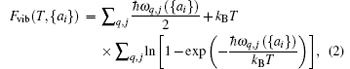
The phonon calculations are performed by using the supercell method through the PHONOPY code, [31] and the real-space force constants of supercells are calculated by using the density-functional perturbation theory (DFPT) as implemented in VASP. In our calculations, the nonanalytic contribution to the dynamical matrix in the limit q→ 0 is even smaller and is neglected. Then the thermal expansion of MX2 can be calculated by the phonon dispersions based on the QHA. Within the QHA, Helmholtz free energy F(T, {ai}) with respect to all the geometrical degrees of freedom {ai} in a crystal is expressed as[32, 33]
where E({ai}) is the total energy of the solid when all atoms are fixed at their crystalline lattice sites, and the second term on the right-hand side is the vibrational contribution to the Helmholtz free energy, which can be calculated using the relationship[34]
where ω q, j({ai}) indicates the dependence of the phonon frequency on the structural parameters {ai}. For our QHA calculations, necessary routine numerical checks on the reliability of the supercell size are made and supercells containing 4× 4× 1 primitive cells are chosen for all STMDs. Direct minimization of the free energy F(T, {ai}) provides the corresponding equilibrium structure at temperature T and zero pressure. So their linear thermal expansions are easily obtained as a variation in the equilibrium lattice constants.
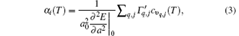
According to Grü neisen theory, the linear thermal expansion coefficient for monolayer MX2 can be given by[24]
where the subscript “ 0” indicates a quantity taken at the ground state lattice parameter. Since cυ q, j(T) is always positive, it is clear that the negative thermal expansion results only from negative values of the Grü neisen parameters for certain phonons. Note that the term in Eq. (3) is equal to 9V0B0 for 3D isotropic crystalline solid.
3. Results and discussion
3.1. In-plane stiffness and charge transfer
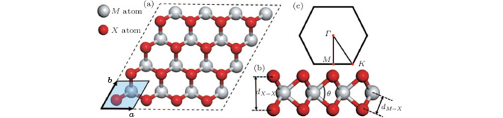
The crystal structure of 2H– MX2 belongs to the point group (space group P63/mmc), and the unit cell consists of six atoms.[35] In contrast, monolayer MX2 belongs to the space group P6m2. The M and X atoms form a hexagonal lattice with trigonal prismatic coordination as depicted in Fig. 1. The calculated structural parameters are listed in Table 1. The data show that the lattice constants of MX2 monolayers of the same X atoms, which are nearly identical, and other lattice parameters, such as the bond angles, change slightly. For MoX2 or WX2, the structural parameters including lattice constants increase significantly with increasing the X atomic radius. Experimental data of the lattice parameters of monolayer STMD are not available yet. However, our calculated lattice constants are close to those of their bulk counterparts. For example, the optimized lattice constant of the MoS2 is 3.19 Å , which is almost the same as the experimental value (3.16 Å )[36] of 2H– MoS2.
Fig. 1. (a) Top and (b) side views of the atomic structure of monolayer MX2. The figure shows a 4× 4 supercell, and the primitive unit cell with lattice vectors a and b (| a| = | b| ) is highlighted by a parallelogram. The relevant internal structural parameters are also indicated. (c) Corresponding Brillouin zone with some high-symmetry points.
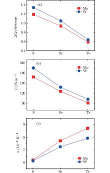
For the single layer MX2, the in-plane stiffness C mentioned above can be given as[37] 1/A0(∂ 2ES/∂ ε 2), where ES is the strain energy calculated by subtracting the total energy at zero strain from the total energy at a given strain (ES = Eε − Eε = 0), and ε is the in-plane uniaxial strain (ε = Δ a/a). In Table 1, in-plane stiffness and the charge transfers of metals for these monolayer semiconductors are also presented. Using the Bader analysis, [38] the charge transfer from the metal to the chalcogen atom is obtained. For MoX2 or WX2, the charge transfer decreases with increasing the row number of the X atom. Generally, the higher the charge transfer, the larger the in-plane stiffness is. Thus the in-plane stiffness decreases with increasing the row number of X. Moreover, the in-plane stiffness of WX2 is usually higher than those of MoX2.
Table 1.
Table 1.
Table 1. Calculated values of lattice constant a, bond lengths (dM− X and dX − X), X– M– X bond angle θ , in-plane stiffness C, and charge transfer of metal Δ Q for monolayer STMD.
a/Å
dM− X/Å
dX− X/Å
θ /(° )
C/(N/m)
Δ Q/electrons
MoS2
3.191
2.418
3.134
80.758
168.15
1.19
MoSe2
3.327
2.547
3.345
82.097
125.34
0.94
MoTe2
3.557
2.737
3.620
82.792
91.38
0.59
WS2
3.194
2.423
3.145
80.927
194.95
1.34
WSe2
3.326
2.552
3.363
82.418
138.04
1.05
WTe2
3.560
2.743
3.632
82.926
102.17
0.64
Table 1. Calculated values of lattice constant a, bond lengths (dM− X and dX − X), X– M– X bond angle θ , in-plane stiffness C, and charge transfer of metal Δ Q for monolayer STMD.
3.2. Phonon
Phonons play a crucial role in determining the thermodynamic properties of crystal. Before determining the thermal expansion of monolayer STMD, it is imperative to investigate their vibrational properties systematically. Since monolayer MX2 has three atoms per primitive cell and is given by point group D3h, besides three acoustic modes, six optical modes at the BZ center are therefore expected. Several studies on their vibrational properties have been reported. For example, Najmaei et al.[39] examined the temperature dependences of the MoS2 vibrational modes with thickness values ranging from a single layer to a few layers. They demonstrated that thermal expansion plays a significant role in determining the temperature dependence of the out-of-plane mode A1g, corresponding to the mode of the monolayer MoS2.
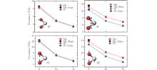
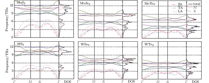
Figure 2 shows the calculated phonon dispersion curves for monolayer MX2 along the high-symmetry points in the first BZ. The calculated acoustical and optical branches of monolayer STMD are positive for any point in BZ, indicating that these suspended, monolayer MX2 compounds are stable. As a characteristic feature of the phonon dispersion of layered crystals, the out-of-plane acoustical (ZA) mode of monolayer MX2 displays a parabolic dispersion because the transverse force decays exponentially, in contrast to the in-plane longitudinal acoustic (LA) and transverse acoustic (TA) branches showing linear dispersions near the Γ point. From Fig. 2, it is clear that the widths of the acoustical and optical branches of MoX2 or WX2 decrease with increasing the row number of the X atom. This is mainly because the strength of the M– X bond reduces as the mass of the X atom increases.
Fig. 2.Ab initio calculations of phonon dispersion curves along the Γ – M– K– Γ direction of the BZ, and vibrational density of states (DOS) for monolayer MX2 at the equilibrium volume. All branches are presented with sharing the same scale of frequency. All acoustical modes (ZA, TA, and LA) as well as vibrational DOS are shown using the same graph legend.
In order to understand clearly their vibrational properties, the frequencies and the corresponding atomic displacements of the optical modes ( at the Γ point are plotted in Fig. 3. For E″ and modes, which are associated with the motions of chalcogen atoms, the vibrational frequencies are determined just by the strength of the M– X bonding. So these modes for WX2 are shifted toward higher frequencies with respect to the MoX2 frequencies. However, the opposite results are obtained for E′ and modes involving the vibrations of both metal and chalcogen atoms, as a result of the heavy metal atom in WX2. Additionally, in Fig. 3, the available experimental data[35, 40, 41] are also presented for comparison. Considering the fact that PBE tends to underestimate the phonon frequencies, the experimental data are well reproduced by our calculations.
Fig. 3. Frequencies of the optical modes at Γ -point for monolayer STMD. Experimental data are cited from Refs. [35], [40], and [41]. The insets show the symmetry representations and the corresponding atomic displacements.
3.3. Thermal expansion
To understand further the contributions of the various modes to thermal expansion, the Grü neisen parameters corresponding to different phonon modes for the monolayer MX2 and those in some high-symmetry directions are shown in Fig. 4. A generalized Grü neisen parameter can be given by[42], which expresses the Grü neisen parameter as a response of the frequency to thermal strain. From the figure, the Grü neisen parameters for the high-frequency optical branches show very little change in a range between 0 to ∼ 1. For MoS2 and WS2, there are quite strong inter-atomic forces, as revealed by the in-plane stiffness. So their acoustical branches are not strongly affected by the thermal strain, that is, the responses (Grü neisen parameters) do not change much. However, for the other MoX2 or WX2 exhibiting relatively small in-plane stiffness, the Grü neisen parameters for these branches are more scattered as the chalcogen atoms go from Se to Te. Interestingly, for MoTe2 and WTe2, some parameters for LA and TA modes ultimately become negative.
Fig. 4. Calculated mode Grü neisen parameters for monolayers of (a) MoX2 and (b) WX2. In panels (a) and (b), the mode Grü neisen parameters as a function of frequency are presented in the first row, and these values along high-symmetry directions are in the second row. All the mode Grü neisen parameters of the optical phonons are shown without graph legend.
In contrast to graphene, [24] in all the monolayer STMDs only a few Grü neisen parameters for the out-of-plane ZA modes are negative, and most are positive. Based on the Bader analysis shown in Table 1, charge transfer gives rise to an excess charge around chalcogen atoms. Consequently, monolayer MX2 can be viewed as a positively charged metal plane sandwiched between two negatively charged planes of chalcogen atoms. Intuitively, this special sandwich structure forms a strong intra-layer interaction, thus will suppress the so-called membrane effect that can be envisioned as bending induced contraction of the layer. So it is not surprising that the monolayer MX2 crystals only have a few negative Grü neisen parameters for the ZA modes. Also, it is not difficult to speculate that their thermal expansion coefficients will be negative at extremely low temperatures.
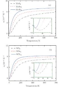
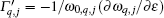
It is indeed shown in Fig. 5 that the linear thermal expansion coefficients for monolayer STMDs exhibit the expected small thermal contractions only in a low-temperature region. The data for MoS2 and MoSe2 obtained by our implementation are in excellent agreement with the reported results.[43] For MoS2, showing the maximum thermal contraction among these compounds, the lattice length decreases gradually as the temperature increases from 0 to 31 K. The minimum value of the linear thermal expansion coefficient is − 2.0× 10− 7K− 1 and occurs at T = 15 K. In this low temperature region the bending modes, which possess very low energy, are responsible for the thermal contraction. At T = 31 K, the lattice length is smallest, and then the thermal contraction turns to an expansion. From 31 K to ∼ 300 K, where more high-energy optical modes are excited, α i(T) increases rapidly with increasing the temperature. Above 300 K this value begins to increase very slowly. For MoTe2 and WTe2, their thermal contractions are relatively small and occur only at T < 9 K and T < 6 K respectively. Moreover, the monolayer STMDs are important in illustrating the general thermal expansion phenomenon in 2D materials.
Fig. 5. Calculated thermal expansions in monolayers of (a) MoX2, and (b) WX2.
When the monolayer MX2 is under an in-plane uniaxial strain arising from thermalization, a useful equation can be expressed as
According to Eq. (3), the linear thermal expansion coefficient in terms of the in-plane stiffness C can be written as
Therefore, α i(T) varies inversely with respect to the in-plane stiffness C for monolayer MX2. However, the negative thermal expansion of monolayer MX2 is the result of the bending effect, and is hardly affected by the in-plane stiffness. So equation (5) is not applicable to the negative thermal expansion of monolayer MX2.
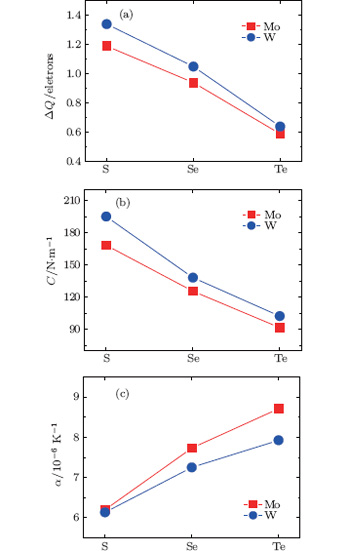
Figure 6 shows the variations of charge transfer of metal, in-plane stiffness, and linear thermal expansion coefficients at 300 K for the monolayer STMDs. For MoX2 and WX2, as the chalcogen atoms go from S, Se, to Te, the trends of variation of their thermal expansions are contrary to those of the in-plane stiffness and charge transfers. Moreover, the linear thermal expansion coefficient of WX2 is a little smaller than that of MoX2, because the former possesses a larger in-plane stiffness. Clearly these calculated results well validate Eq. (5) and the relevant discussion mentioned above. In summary, the effects of in-plane stiffness and charge transfers on the thermal expansions of the monolayer STMDs are further clarified. The differences in their positive thermal expansions are determined mainly by the in-plane stiffness. Indeed, these differences can be attributed to the fundamental difference in the level of charge transfer from M to the X atom. In the case of negative thermal expansion, the discrepancies may be due to the difference in bending stiffness among the monolayer STMDs.
Fig. 6. Variations of (a) charge transfers of metal Δ Q, (b) in-plane stiffness C, and (c) linear thermal expansion coefficient α at 300 K for monolayer STMDs.
4. Conclusions
First-principles phonon calculations clearly show the interrelationships among the thermal expansions, in-plane stiffness, and charge transfers in monolayer STMDs. The thermal contraction of monolayer MX2 is very small and appears only at extremely low temperatures. The mode Grü neisen parameters show that the ZA bending acoustic modes are responsible for the contraction, in a direct manifestation of the membrane effect. Their positive thermal expansion coefficients follow the order of MoX2 > WX2 and MS2 < MSe2 < MTe2. These changes can be well explained by the equation
That is, α i(T) varies inversely with the in-plane stiffness C. Essentially, the difference in their positive thermal expansions can be attributed to the fundamental differences in charge transfer from M to the X atom. The observation is beneficial to the practical applications of STMDs and the understanding of the thermal stability of other 2D systems.
Acknowledgment
One of the authors (Z. Y. Wang) is grateful to professor Wang Song-You in Fudan University for their helpful discussion. The calculations were performed on the High Performance Clusters of Zhengzhou University.
ShiY, ZhouW, LuA Y, FangW, LeeY H, HsuA L, KimS M, KimK K, YangH Y, LiL J, IdroboJ C and KongJ2012Nano Lett. 122784DOI:10.1021/nl204562j[Cited within:1][JCR: 13.025]
... [1] In the quasi-harmonic approximation (QHA), the thermal expansion coefficient[2] for a three-dimensional (3D) crystal is equal to (1/BV)#cod#x2211 ...
1
2014
1.148
1.2429
... [1] In the quasi-harmonic approximation (QHA), the thermal expansion coefficient[2] for a three-dimensional (3D) crystal is equal to (1/BV)#cod#x2211 ...
1
2006
3.842
0.0
... [3#cod#x2013 ...
1
2010
3.794
0.0
1
2011
0.0
0.0
... 5] Owing to sharing the same hexagonal lattice, the monolayer semiconducting transition metal dichalcogenide (STMD) is an ideal prototype to determine the correlation between thermal expansion and in-plane stiffness ...
Ultrathin two-dimensional nanosheets of layered transition metal dichalcogenides (TMDs) are fundamentally and technologically intriguing. In contrast to the graphene sheet, they are chemically versatile. Mono-or few-layered TMDs - obtained either through exfoliation of bulk materials or bottom-up syntheses - are direct-gap semiconductors whose bandgap energy, as well as carrier type (n- or p-type), varies between compounds depending on their composition, structure and dimensionality. In this Review, we describe how the tunable electronic structure of TMDs makes them attractive for a variety of applications. They have been investigated as chemically active electrocatalysts for hydrogen evolution and hydrosulfurization, as well as electrically active materials in opto-electronics. Their morphologies and properties are also useful for energy storage applications such as electrodes for Li-ion batteries and supercapacitors.
... [9,16,17] However, the performance of the complex MX2-based devices will change significantly due to internal stresses imposed by different expansion coefficients ...
1
2011
3.842
0.0
1
2013
12.062
0.0
1
2014
1.148
1.2429
1
2012
13.025
0.0
1
2013
14.829
0.0
... 14] For instance, monolayer MoS2, a prototypical example of STMD with a large intrinsic direct bandgap of #cod#x223C ...
1
2010
7.943
0.0
... 8 eV,[15] is a very desirable candidate for optoelectronics and digital electronics with thermal stability up to 1100 ...
1
2013
31.17
0.0
... [9,16,17] However, the performance of the complex MX2-based devices will change significantly due to internal stresses imposed by different expansion coefficients ...
1
2012
13.025
0.0
... [9,16,17] However, the performance of the complex MX2-based devices will change significantly due to internal stresses imposed by different expansion coefficients ...
1
2004
7.943
0.0
... [18#cod#x2013 ...
1
2011
13.025
0.0
1
2010
3.842
0.0
1
2009
0.0
0.0
... 21] In addition, according to the ubiquitous membrane effect,[22,23] the ZA bending acoustic modes may cause negative thermal expansion in membranes or layered materials ...
1
1982
1.534
0.0
... 21] In addition, according to the ubiquitous membrane effect,[22,23] the ZA bending acoustic modes may cause negative thermal expansion in membranes or layered materials ...
1
2002
4.0
0.0
... 21] In addition, according to the ubiquitous membrane effect,[22,23] the ZA bending acoustic modes may cause negative thermal expansion in membranes or layered materials ...
3
2005
0.0
0.0
... [24] Thus, the monolayer STMD is also expected to contract at some specific temperatures ...
... neisen theory, the linear thermal expansion coefficient for monolayer MX2 can be given by[24] ...
... In contrast to graphene,[24] in all the monolayer STMDs only a few Gr#cod#x00FC ...
1
1979
3.343
0.0
... Unlike the corresponding bulk material,[25] monolayer MX2 shows a negative thermal expansion (NTE) at low temperatures ...
1
1996
1.878
0.0
... [26#cod#x2013 ...
1
1996
0.0
0.0
1
1999
0.0
0.0
... 28] The projector-augmented wave function (PAW) method[29] with the Perdew#cod#x2013 ...
1
1994
0.0
0.0
... 28] The projector-augmented wave function (PAW) method[29] with the Perdew#cod#x2013 ...
1
1996
7.943
0.0
... Ernzerh[30] (PBE) of generalized gradient approximation (GGA) is adopted ...
1
2008
0.0
0.0
... The phonon calculations are performed by using the supercell method through the PHONOPY code,[31] and the real-space force constants of supercells are calculated by using the density-functional perturbation theory (DFPT) as implemented in VASP ...
1
2012
1.148
1.2429
... Within the QHA, Helmholtz free energy F(T,{ai}) with respect to all the geometrical degrees of freedom {ai} in a crystal is expressed as[32,33] ...
1
2013
0.71
0.0
... Within the QHA, Helmholtz free energy F(T,{ai}) with respect to all the geometrical degrees of freedom {ai} in a crystal is expressed as[32,33] ...
1
2008
0.0
0.0
... where E({ai}) is the total energy of the solid when all atoms are fixed at their crystalline lattice sites, and the second term on the right-hand side is the vibrational contribution to the Helmholtz free energy, which can be calculated using the relationship[34] ...
2
2010
0.0
0.0
... [35] In contrast, monolayer MX2 belongs to the space group P6m2 ...
... 3, the available experimental data[35,40,41] are also presented for comparison ...
1
2003
0.0
0.0
... )[36] of 2H#cod#x2013 ...
1
2011
4.814
0.0
... For the single layer MX2, the in-plane stiffness C mentioned above can be given as[37] 1/A0(#cod#x2202 ...
Abstract An algorithm is presented for carrying out decomposition of electronic charge density into atomic contributions. As suggested by Bader [R. Bader, Atoms in Molecules: A Quantum Theory, Oxford University Press, New York, 1990], space is divided up into atomic regions where the dividing surfaces are at a minimum in the charge density, i.e. the gradient of the charge density is zero along the surface normal. Instead of explicitly finding and representing the dividing surfaces, which is a challenging task, our algorithm assigns each point on a regular ( x , y , z ) grid to one of the regions by following a steepest ascent path on the grid. The computational work required to analyze a given charge density grid is approximately 50 arithmetic operations per grid point. The work scales linearly with the number of grid points and is essentially independent of the number of atoms in the system. The algorithm is robust and insensitive to the topology of molecular bonding. In addition to two test problems involving a water molecule and NaCl crystal, the algorithm has been used to estimate the electrical activity of a cluster of boron atoms in a silicon crystal. The highly stable three-atom boron cluster, B 3 I is found to have a charge of −1.5 e, which suggests approximately 50% reduction in electrical activity as compared with three substitutional boron atoms.
... Using the Bader analysis,[38] the charge transfer from the metal to the chalcogen atom is obtained ...
Raman spectroscopy is utilized to quantify the temperature dependency of the vibrational modes in molybdenum disulfide (MoS2) atomic layers. These analyses are essential for understanding the structural properties and phononic behaviors of this two-dimensional (2D) material. We quantitatively analyze the temperature dependent shifts of the Raman peak positions in the temperature range from 300 to 550 K, and find that both planar and out-of-plane characteristic modes are highly sensitive to temperature variations. This temperature dependency is linear and can be fully explained by the first-order temperature coefficient. Using a semi-quantitative model, we evaluate the contributions of the material's thermal expansion and intrinsic temperature effects to this dependency. We reveal that the dominating source of shift in the peak position of planar mode E-2g(1) for samples of all thicknesses investigated is the four-phonon process. In addition to the four-phonon process, thermal expansion plays a significant role in the temperature dependency of the out-of-plane mode, A(1g). The thickness dependency of the temperature coefficient for MoS2 and a drastic change in behaviors of samples from bi- to single-layered are also demonstrated. We further explore the role of defects in the thermal properties of MoS2 by examining the temperature dependency of Raman modes in CVD-grown samples.
Najmaei, Sina 1 ;Ajayan, Pulickel M. 1 ;Lou, J. 1 ;
... [39] examined the temperature dependences of the MoS2 vibrational modes with thickness values ranging from a single layer to a few layers ...
1
2010
12.062
0.0
... 3, the available experimental data[35,40,41] are also presented for comparison ...
1
2013
0.0
0.0
... 3, the available experimental data[35,40,41] are also presented for comparison ...
1
2003
0.0
0.0
... neisen parameter can be given by[42], which expresses the Gr#cod#x00FC ...
1
2014
0.0
0.0
... [43] For MoS2, showing the maximum thermal contraction among these compounds, the lattice length decreases gradually as the temperature increases from 0 to 31 K ...
Effects of in-plane stiffness and charge transfer on thermal expansion of monolayer transition metal dichalcogenide*
[Wang Zhan-Yua),b), Zhou Yan-Lic), Wang Xue-Qingb), Wang Feia),b), Sun Qianga),b), Guo Zheng-Xiaoa),b),d), Jia Yua),b)†]


 ]
]