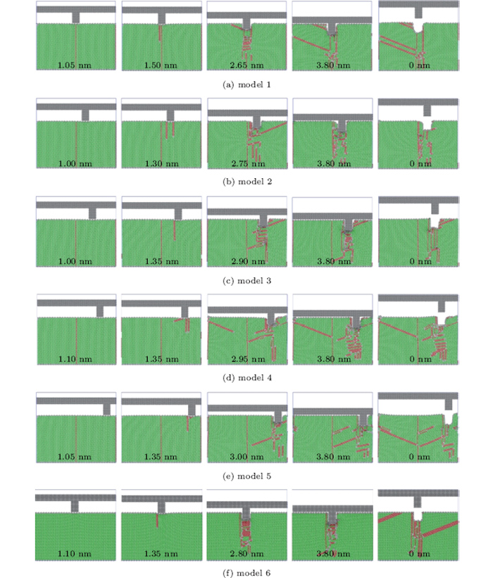
Effect of twin boundary on nanoimprint process of bicrystal Al thin film studied by molecular dynamics simulation*
Xie Yue-Honga)†, Xu Jian-Ganga), Song Hai-Yangb)‡, Zhang Yun-Guanga)
       
Instantaneous defect structures of bicrystal Al thin film and single crystal with different mould displacements when the TB direction is parallel to the imprinting direction at 0.01 K obtained by our MD simulation. Five kinds of mark intervals are used: (a) 10.1 nm, (b) 11.7 nm, (c) 13.7 nm, (d) 15.7 nm, (e) 17.7 nm; (f) single crystal.