


Effect of twin boundary on nanoimprint process of bicrystal Al thin film studied by molecular dynamics simulation*
[Xie Yue-Honga)†  , Xu Jian-Gang
a) , Song Hai-Yangb)‡ , Zhang Yun-Guanga) ]
, Xu Jian-Gang, Zhang Yun-Guang|
|


Corresponding author. E-mail: lengyue204@163.com
Corresponding author. E-mail: gsfshy@sohu.com
Project supported by the National Natural Science Foundation of China (Grant No. 10902083), the Program for New Century Excellent Talent in University of Ministry of Education of China (Grant No. NCET-12-1046), the Program for New Scientific and Technological Star of Shaanxi Province, China (Grant No. 2012KJXX-39), and the Program for Natural Science Basic Research Plan in Shaanxi Province, China (Grant No. 2014JQ1036).
The effects of a twin boundary (TB) on the mechanical properties of two types of bicrystal Al thin films during the nanoimprint process are investigated by using molecular dynamics simulations. The results indicate that for the TB direction parallel to the imprinting direction, the yield stress reaches the maximum for the initial dislocation nucleation when the mould directly imprints to the TB, and the yield stress first decreases with the increase of the marker interval and then increases. However, for the TB direction perpendicular to the imprinting direction, the effect of the TB location to the imprinting forces is very small, and the yield stress is greater than that with the TB direction parallel to the imprinting direction. The results also demonstrate that the direction of the slip dislocations and the deformation of the thin film caused by spring-back are different due to various positions and directions of the TB.
Nanoimprint lithography (NIL), first reported by Chou et al. in 1995, [1] is a direct nanoimprint technology. NIL manufactures a nanopattern by pressing a hard mould with the nanopattern into a thin film and making the film produce a mechanical deformation.[2] Nanoimprint is very valuable for making some nanostructures under proper pressure and temperature.[3– 5] Besides that, it has the advantages of low cost, short cycle time, high replication, and high resolution.[6, 7] Therefore, NIL has been widely used in the manufacture of semiconductors, optoelectronics, and biological nanomaterials for excellent performance.[8, 9]
Molecular dynamics (MD) simulation is a powerful tool for investigating material behaviors at the nanoscale, so a lot of researches have been carried out with MD.[10– 14] Hsu et al.[15, 16] and Cheng et al.[17] first used the MD simulation to study the nanoimprint process. Since numerical simulations can be applied efficiently to deal with the deformation behavior of a material during the nanoimprint process, several studies using the MD simulation were performed.[18– 20] Process parameters such as temperature, mould velocity, and spring-back were investigated for copper nanoimprint by Hsu et al.[16] They found that the needed imprinting force decreases with the increase of temperature, but it increases with the increase of loading velocity. Besides, their results showed that the spring-back of a horizontal deformed atomic crystal moves more seriously than in the vertical direction when the punch leaves the specimen. The effects of the punch position and the alloy components of the Cu– Ni alloy on the nanoimprint process were studied through MD simulation by Fang et al.[21] They found that the imprinting force of the specimen increases with the increase of punch position and the decrease of Ni content. In addition, the spring-back phenomenon was more obvious with the increase of Ni content after the mould was retrieved during the nanoimprint behavior. The void effects on the nanoimprint process of single crystal Al thin film were studied by Yuan et al.[22] The results showed that the needed maximum force for the initial dislocation nucleation increases with the decrease of the void volume fraction. Furthermore, they also found that the plastic deformation was influenced by the void volume fraction and the dislocation activity. The effects of stamp spacing on the nanoimprint process of bicrystal Al with twin boundary (TB) were demonstrated by He et al.[23] The results indicated that the plastic deformation modes of bicrystal Al thin film include dislocation activity and dislocation– TB interaction. Moreover, they found that the stamp spacing had a significant influence on the dislocation– TB interaction. The previous simulation works have examined the possible mechanisms of TB under various loading conditions of tension, indentation, and bending.[24, 25] Nevertheless, the related discussion concerning the effect of the TB during a nanoimprint process is still very rare. Here, we investigate the effect of TB on the mechanical behavior of bicrystal Al thin film during the nanoimprint process by using the MD simulation.
The rest of the present paper is organized as follows. In Section 2, we outline the method and models that we chose for our study. The results and discussion are shown in Section 3. The conclusions from the present study are provided in Section 4.
In order to investigate the influence of the TB in a nanoimprint process, we use two types of specimens, as indicated in Fig. 1. In both of the models, the simulation models for the nanoimprint process include a bicrystal Al thin film and a Si mould. The surface crystal orientations of the bicrystal Al thin film in the two models are 
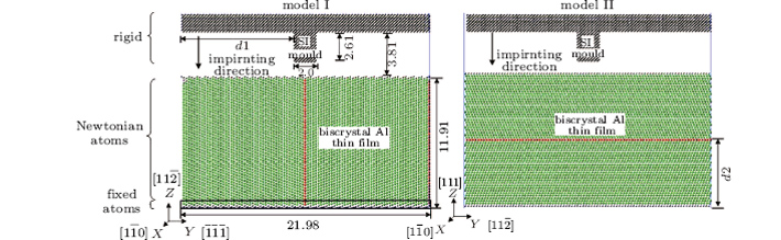 | Fig. 1. Initial models for MD simulation (dimensions are given in units of nm): (a) model I represents the specimen with the TB direction parallel to the imprinting direction, (b) model II represents the specimen with the TB direction perpendicular to the imprinting direction. |
The accuracy of the results in the MD simulation depends on the selection of the potential function. Due to the fact that the hardness of Si is far greater than Al, the deformation of the Si mould and the interactions between Si– Si atoms can be neglected. We are only concerned with Al– Al and Al– Si interactions in theory. Here, the embedded atom method (EAM) potential, which is more accurate in the computation of the interaction between metals, is applied to describe the interactions between the Al– Al atoms.[26– 28] The Lennard-Jones potential is used to analyze the interaction between the Al– Si atoms, [29] and the cut-off radius is 1.02 nm.[22] For the purpose of comparision, a single crystal Al thin film with the same configuration is also considered in simulations. The Verlet algorithm is applied to integrate the equations of motion. A time step of 1 fs is used in the present simulations. In order to minimize the system energy, two types of models are equilibrated for 2 ps in the NVT ensemble before nanoimprint simulations.[30] The temperature of 0.01 K is used during the whole simulation. The simulation is divided into loading and unloading stages. The loading stage lasts for 76 ps and the final mould displacement is 3.80 nm (2.60-nm imprinting depth). It takes 38 ps for moving the same length in the unloading stage. The velocities of two stages are 50 m/s and 100 m/s, respectively. With the purpose of discerning defects in the bicrystal Al thin film, the common neighbor analysis (CNA) is used to determine each part of instantaneous crystal structure of the thin film.[31] The Open Visualization Tool (OVITO), [32] which is analyzing and classifying the environment around each atom, is implemented to identify various deformation mechanisms during the nanoimprint process.
We first investigate the effect of TB when the TB direction is parallel to the imprinting direction. Figure 2 presents the force versus the mould moving distance obtained in the nanoimprint of a bicrystal Al thin film using five kinds of marker intervals and a single crystal. At the beginning of the loading stage, we can see that the force is zero and lasts a period of time. Then, due to an attractive force between the mould bottom and the bicrystal Al thin film, which is due to the very short distance between them, the force turns into a negative one. Figure 3 displays a set of snapshots which show the evolution of imperfections in the bicrystal and the single crystal Al thin films at various moving distances. The attractive phenomenon can be seen in the first pictures of Figs. 3(a)– 3(f); when the mould bottom compresses the Al thin film, the thin film surface bends without generating any dislocations. It indicates that the thin film undergoes purely elastic deformation. Whereafter, the imprinting force of models 1– 5 firstly presents a linear growth and reaches the yield stress of the thin film, which are 35.56 nN, 16.06 nN, 15.12 nN, 18.72 nN, and 19.40 nN at the mould displacements of 1.50 nm, 1.25 nm, 1.25 nm, 1.30 nm, and 1.35 nm, respectively, as shown in Fig. 2. The nucleation of the initial dislocation from the contact area under both sides of the mould bottom is observed, as illustrated in the second column of Figs. 3(a)– 3(e). That is, the first partial dislocation nucleates at the nanoimprinting surface, signaling the initiation of yielding.[33] At the same time, the imprinting force of models 1– 5 ceases increasing and drops slightly, as shown in the first inset of Fig. 2. This is a symbol of plastic deformation. Subsequently, the imprinting force of models 2– 5 increases rapidly again (similar to that in model 1), where the force increases from 14.25 nN, 15.11 nN, 16.73 nN, and 17.59 nN to 29.72 nN, 26.63 nN, 20.52 nN, and 31.39 nN during mould moving from 1.30 nm, 1.35 nm, 1.35 nm, and 1.40 nm to 1.45 nm, 1.55 nm, 1.40 nm, and 1.60 nm, respectively. These upsurges of the imprinting force coincide with the local accumulation and stacking of dislocations under the mould. When the imprinting force reaches the critical value, which is large enough to overcome the plastic deformation resistance, the dislocations become very active, as shown in the third column of Figs. 3(a)– 3(e), which create hardening effects in the bicrystal Al thin film. Then, the imprinting force of models 1– 5 has very obvious repeated drops with a very small increase during a long period, which shows that stick-slip occurs during the deformation. The fluctuation phenomenon associated with the force is caused by successive dislocation nucleation events. At the final period of the loading process, the imprinting forces of all models have a large increase, which is caused by the contact of the inside top surface of the mould with the thin film surface. The peak forces of models 1– 5 are 127.99 nN, 128.63 nN, 105.16 nN, 112.28 nN, and 95.43 nN, respectively, as shown in the second inset of Fig. 2. Meanwhile, the dislocation density of the thin film increases greatly until reaching the desired mould displacement of 3.80 nm, as revealed in the fourth column of Figs. 3(a)– 3(e). The following unloading stage is defined as the mould gradually separates from the thin film to its initial position. With the increase of the total relaxation time, the high energy of the thin film reduces, the imprinting force dramatically falls and decreases further to zero, as shown in Fig. 2, and part of the slip dislocations disappear along the opposite direction of the slip plane. The pressed area of the thin film under the mould bottom has an obvious spring-back behavior in the vertical direction (the Z direction), [34] in complete contrast to snapshots at the mould displacement of 3.80 nm, as shown in the last column of Figs. 3(a)– 3(e). On the other hand, the imprinting surface is not so perfect due to this spring-back phenomenon. This result is in agreement with the previous study by Pei et al.[18]
 | Fig. 2. The imprinting force varies with the mould displacement on single crystal and bicrystal Al thin film using five kinds of mark intervals when the TB direction is parallel to the imprinting direction at 0.01 K. Model 6 uses a single crystal. For models 1– 5, the mark intervals are 10.1 nm, 11.7 nm, 13.7 nm, 15.7 nm, and 17.7 nm, respectively. |
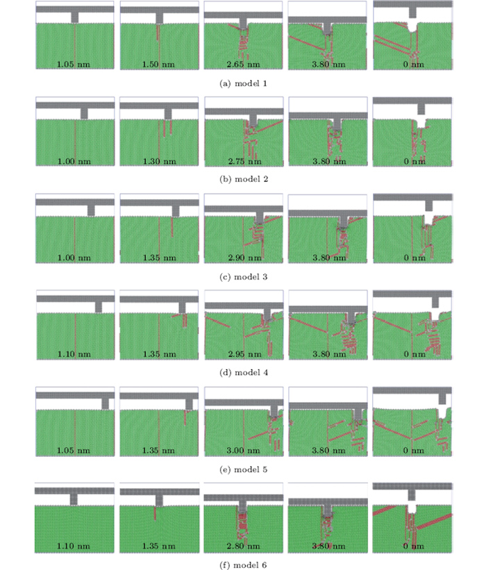 | Fig. 3. Instantaneous defect structures of bicrystal Al thin film and single crystal with different mould displacements when the TB direction is parallel to the imprinting direction at 0.01 K obtained by our MD simulation. Five kinds of mark intervals are used: (a) 10.1 nm, (b) 11.7 nm, (c) 13.7 nm, (d) 15.7 nm, (e) 17.7 nm; (f) single crystal. |
Comparing the imprinting force curves of models 1– 5, it can be seen that the yield stress of model 1 is maximum for the initial dislocation nucleation from the first inset in Fig. 2. This may be because that the mould directly acts on the TB, the emitted dislocations are close to the TB, and the hardness of the material is larger due to the imprinting direction parallel to the close-arranged plane.[35] Besides, it is observed that the yield stress first decreases with the increase of the marker interval and then increases. This result may be due to the strong competition between the stress offered by the mould and that offered by the centered and righted TB.[23] When the imprinting position of the mould is close to the TB, the required yield stress is larger. At the final period of the loading stage, the peak force of model 1 is approximately equal to that of model 2. Meanwhile, in addition the force in model 4 is greater than that in model 3, the peak force decreases with the increase of the marker interval, as shown in the second inset of Fig. 2. This phenomenon may be attributed to the interaction between the launch of dislocation and the TB. As a comparison, a single crystal Al thin film with the same crystallographic orientation is also investigated. Figure 2 also shows the yield stress of the single crystal and that the peak force is greater than that in the bicrystal Al thin film. The disagreement between the single crystal and the bicrystal Al thin film can be attributed to the TB. It indicates that pre-existing TB defects can lower the yield stress required for the homogeneous nucleation of the dislocation from the imprinted surface.[23]
The influence of the TB for the dislocation nucleation and movement can be seen from Fig. 3. The distances of models 2 and 3 to the centered TB are equal to those of models 5 and 4 to the righted TB, respectively. The dislocation movements in models 2 and 3 are hindered by the centered TB, which leads to the occurrence of work hardening in the bicrystal Al thin film.[36] However, as the dislocations in models 4 and 5 go across the righted TB and continue to slip, a stacking fault can be observed in the left side of the centered TB at the mould displacement of 3.8 nm. In addition, it can be seen that the centered TB disappears in model 1, while a new TB appears under the left side of the mould bottom and the dislocations slip to the left. The above observation indicates that the dislocation slip easily occurs in the left side of the centered TB. As shown in the snapshots of model 6, after nucleation, the dislocations stack under the mould and a new TB appears in the single crystal Al thin film, which hinders the dislocation glide and causes work hardening of the material. Besides, we can see that model 6 is very similar to model 2 when the mould displacement is 3.80 nm. The result shows that the nanoimprint of single crystal amounts to the mould being close to the TB. At the unloading stage, the phenomenon of dislocation slip is obvious due to the spring-back. Figures 3(a)– 3(f) show that the slip dislocations are in a small angle or parallel to the imprinting direction. Researches have pointed out that deformation twinning cannot easily occur in high stacking fault energy FCC metals.[37] However, it is interesting that some deformation twinning is observed in the unloading process, as shown in Fig. 3. This may be due to that part of the energy is released and there are obvious TBs in the vertical direction in model 3 associated with the spring-back.[38] Furthermore, the deformation mechanism may be also due to the high loading rate and the quasi-three-dimensional model in the width direction, which restricts the activation of multiple slip systems.[34] This result is coincident with the fact that the deformation twinning is another plastic deformation of the FCC structure.[39]
Now we examine the effect of TB when the TB direction is perpendicular to the imprinting direction. Here, MD simulations are carried out for three kinds of TB locations in the Al thin film. Furthermore, for comparison, both the deformation behavior and the mechanical response of a single crystal Al thin film are also taken into account during the nanoimprint.
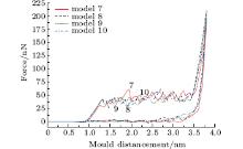
The simulated imprinting forces during the nanoimprint process for the Al thin film with the TB and the single crystal are shown in Fig. 4, along with the mould moving distance. It can be seen from the imprinting force curves that the several stage deformation also exists for the nanoimprint in models 7– 10. However, the imprinting forces for different TB directions show some differences. One difference is that the imprinting forces of models 8– 10 without increasing rapidly again after reaching the maximum yield stress are 42.10 nN, 41.95 nN, and 41.91 nN, respectively. Another difference is that the imprinting forces of models 8– 10 are almost plateaued with a very small increase in a long period, which shows that stick-slip is not particularly obvious during the deformation. Figure 5 displays a set of MD simulation snapshots employing different TB locations and the single crystal, which show that the evolution of imperfections in the bicrystal and the single crystal Al thin films at various moving distances. The simulation results show that the Al thin film in models 7– 10 undergoes a similar deformation process to that in models 1– 5. At the initial stage of nanoimprinting, no dislocations are formed and the deformation is purely elastic, as illustrated in the first column of Figs. 5(a)– 5(d). In the second column, the dislocations begin to nucleate in the Al thin film and thus the plastic deformation occurs. Then, a large amount of dislocations are generated and piled up until reaching the desired mould displacement of 3.80 nm, as revealed in the fourth column. Finally, at the unloading stage, an obvious spring-back behavior appears in the vertical direction.
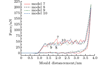 | Fig. 4. The imprinting force varies with the mould displacement on single crystal and bicrystal Al thin film with different TB locations when the TB direction is perpendicular to the imprinting direction at 0.01 K. Model 7 is for the single crystal. In models 8– 10, the distances between the TB and the XOY plane are 9.12 nm, 6.31 nm, and 3.51 nm, respectively. |
 | Fig. 5. Instantaneous defect structures of single crystal and bicrystal Al thin film with different mould displacements when the TB direction is perpendicular to the imprinting direction at 0.01 K obtained by MD simulations: (a) single crystal; the distances between the TB and the XOY plane are (b) 9.12 nm, (c) 6.31 nm, and (d) 3.51 nm. |
Comparing the imprinting force curves of the four models in Fig. 4, we can see that the curves obtained for models 9 and 10 are very similar to that for model 8. This result shows that the TB location has little effect on imprinting forces when the imprinting direction is perpendicular to the TB direction. Compared with the yield stresses in models 1– 5, the yield stresses of models 8– 10 shown in Fig. 4 are greater, which may be due to the fact that the hardness of the material is the largest when the imprinting direction is perpendicular to the close-arranged plane. This result is in agreement with the previous study.[35] In addition, at the final period of the loading stage, the peak forces of models 8– 10 are also greater than those of models 1– 5, which is attributed to the fact that the contact areas of models 8– 10 are larger than those of models 1– 5. Here, the contact area refers to the inside top surface of the Si mould and the surface of the Al thin film when the mould displacement is 3.80 nm. The contact area is small because the surface of the Al thin film of models 1– 5 is not flat.[40] Figure 4 also shows that the yield stress of the single crystal is smaller than that of the bicrystal Al thin film, and that the imprinting force of single crystal Al has an increasing process again. The disagreement between the single crystal and the bicrystal Al thin film can be attributed to the TB that hinders the slip dislocations and increases the imprinting force.
For models 8– 10, the dislocation nucleation and movement are also studied and the results are different from those for models 1– 5. The snapshots during the imprinting process for models 8– 10 are shown in Figs. 5(b)– 5(d), in which one can see the dislocations through the TB at the mould displacements of 2.45 nm, 3.05 nm, and 3.5 nm, respectively, as shown in the third column. This result shows that the mould displacement increases with the decrease of the distance between the TB and the XOY plane when the dislocations go across the TB. Moreover, we can see that a large amount of dislocations are hindered by the TB at the mould displacement of 3.8 nm, and the dislocation density increases with the decrease of the distance between the TB and the XOY plane. Thus the TB can hinder the dislocation slip. This phenomenon also appeared in the previous study.[24] During the unloading process, the cross-slip of the stacking fault is observed in model 8 and the TBs along the direction of the slip dislocations are generated in model 10 due to the spring-back. This phenomenon is also observed in model 7. In other words, as the distance between the TB and the imprinted surface gets larger, the TBs at the bottom of the mould are more easily observed on account of the spring-back and energy reduction. For imprint on the (111) surface, figures 5(a)– 5(d) show that the slip dislocations are in a small angle or vertical to the imprinting direction. This result is also consistent with the previous research about the nanoimprint on copper.[18]
MD simulation is performed to study the effect of the TB on the mechanical response and the deformation behavior of two types of bicrystal Al thin films during the nanoimprint process. The results show that there is a significant difference between the distributions of dislocations in the two types of imprinted materials. For the TB direction parallel to the imprinting direction, because the emitted dislocation is close to the TB, the yield stress is maximum for the initial dislocation nucleation when the mould directly imprints to the TB. Furthermore, it can be seen that the yield stress first decreases with the increase of the marker interval and then increases because of the strong competition between the stress offered by the mould and that offered by the centered and righted TB, and the dislocations easily go across the TB on the right side. For the TB direction perpendicular to the imprinting direction, the result indicates that the TB location only slightly affects the imprinting forces and the mould displacement increases with the decrease of the distance between the TB and the XOY plane when the dislocations pass through the TB, this is becasue the TB hinders the slip dislocation. In addition, all models show an obvious phenomenon of spring-back due to the stick-slip during the unloading stage.
| 1 |
|
| 2 |
|
| 3 |
|
| 4 |
|
| 5 |
|
| 6 |
|
| 7 |
|
| 8 |
|
| 9 |
|
| 10 |
|
| 11 |
|
| 12 |
|
| 13 |
|
| 14 |
|
| 15 |
|
| 16 |
|
| 17 |
|
| 18 |
|
| 19 |
|
| 20 |
|
| 21 |
|
| 22 |
|
| 23 |
|
| 24 |
|
| 25 |
|
| 26 |
|
| 27 |
|
| 28 |
|
| 29 |
|
| 30 |
|
| 31 |
|
| 32 |
|
| 33 |
|
| 34 |
|
| 35 |
|
| 36 |
|
| 37 |
|
| 38 |
|
| 39 |
|
| 40 |
|