

Exciplex formation and electroluminescent absorption in ultraviolet organic light-emitting diodes*
[Zhang Qia) , Zhang Haoa) , Zhang Xiao-Wenb)†  , Xu Tao
a) , Wei Bina)‡ ]
, Xu Tao]
|
|


Corresponding author. E-mail: zhang-xiaowen@163.com
Corresponding author. E-mail: bwei@shu.edu.cn
Project supported by the National Natural Science Foundation of China (Grant Nos. 61136003 and 61275041) and the Guangxi Provincial Natural Science Foundation, China (Grant No. 2012GXNSFBA053168).
We investigated the formation of exciplex and electroluminescent absorption in ultraviolet organic light-emitting diodes (UV OLEDs) using different heterojunction structures. It is found that an energy barrier of over 0.3 eV between the emissive layer (EML) and adjacent transport layer facilitates exciplex formation. The electron blocking layer effectively confines electrons in the EML, which contributes to pure UV emission and enhances efficiency. The change in EML thickness generates tunable UV emission from 376 nm to 406 nm. In addition, the UV emission excites low-energy organic function layers and produces photoluminescent emission. In UV OLED, avoiding the exciplex formation and averting light absorption can effectively improve the purity and efficiency. A maximum external quantum efficiency of 1.2% with a UV emission peak of 376 nm is realized.
Organic light-emitting diodes (OLEDs) have received considerable attention due to their superb display image quality and compatibility with large-area, flexible substrates.[1– 3] To date, most research efforts have focused on the development of visible light emitting OLEDs. However, extending the emissions of OLEDs into ultraviolet wavelengths holds unique promise for applications in biological and chemical sensing, information storage, and full-color light-emitting displays.[4– 7] However, the molecular design of amorphous organic materials capable of efficient UV emissions in OLEDs is highly challenging. To achieve a short-wavelength emission a wide band-gap is required and the extent of conjugation in the molecule must be confined. Limiting the conjugation would lead to a strong tendency to destabilize the radical cations and/or radical anions upon electrochemical oxidation.[8, 9] Furthermore, the intrinsic wide band-gap, which counteracts the carrier injection, results in a significant challenge in the design of multilayer UV OLED devices configured to give the highest UV emission.
Most researchers have directed their efforts toward designing and developing novel UV-emitters in a few existing reports on UV OLEDs. Studies on the mechanism of undesired emission, exciplex formation, and optical absorption in UV OLED are rarely available. Particularly, in UV OLED, the energy barrier at the organic interface has a considerable effect on the recombination process. In this work, we investigate a series of azole derivatives-based devices with the purpose of obtaining pure UV emission, and probing the mechanisms of exciplex formation and optical absorption.
We notice that an appropriate energy level alignment plays a crucial role in multilayer ultraviolet OLEDs. Furthermore, the emission spectrum and intensity depend on the thickness of 3-(4-biphenyl)-4-phenyl-5-tert-butylphenyl-l, 2, 4-triazole (TAZ). Finally, the influence of electroluminescent (EL) absorption of organic function layer, which is different from the photoluminescence (PL) absorption of pure film, on emission spectrum is also systematically investigated.
Considering the energy level alignment in a UV OLED, we chose molybdenum oxide (MoO3) as the hole-injecting layer (HIL) sandwiched between tin-doped indium oxide (ITO) and hole-transport layer (HTL).[10– 13] Transition-metal oxide such as MoO3 served as HIL, due to its stability and high work function.[14] The p-type doping of organic semiconductors has been realized by doping MoO3 into organics with deep highest occupied molecular orbital (HOMO) levels, such as 4’ , 4” -Tris(carbazol-9-yl)triphenylamine (TCTA) and 4, 4’ -bis(carbazol-9-yl)biphenyl (CBP).[15– 17] The p-type doped organic results in Ohmic contact between ITO and HTL. The reasons for the Ohmic contact include the formation of charge transfer complexes, the low hole injecting barrier height, and new metal-induced gap states below the Fermi level (EF).[18– 21] It is proven that the MoO3-doped HTL also softens the interfacial energy barrier and enhances hole injection.
We have investigated the effects of hole transport materials (HTMs) by making use of the structure of MoO3 (2 nm)/MoO3-doped HTM (20 nm)/neat HTM (5 nm) as HTL and 1, 3-bis[2-(4-tert-butylphenyl)-1, 3, 4-oxadiazo-5-yl]benzene(OXD-7) (20 nm) as EML. In devices A and B, the CBP and TCTA were used as HTM, respectively. For realizing a pure and high-efficiency UV emission, the other azole derivatives of TAZ and 2-(4-Biphenylyl)-5-phenyl-1, 3, 4-oxadiazole (PBD) served as emitters and were referred to as devices C and D, respectively. Moreover, we investigated the dependences of EL spectra and intensity on the thickness of EML by fabricating devices E, F, and G with TAZ thickness values of 30 nm, 40 nm, and 50 nm, respectively. Finally, the effects of electron transport layer (ETL) on recombination site and optical absorption were investigated. Using OXD-7 as EML, devices H and I with tris-(8-hydroxyquinoline) aluminum (Alq3) and PBD used as ETL, respectively, were fabricated. Using TAZ as EML, we fabricated devices J and K by employing Alq3 and PBD as ETL, respectively.
All of the devices were fabricated by conventional vacuum deposition of the organic layers and cathode onto ITO (15 Ω /sheet, 150 nm) coated glass substrates under a base pressure lower than 1.0 × 10− 5 mbar (1 bar = 105 Pa). Prior to deposition the glass substrates were cleaned with detergent, de-ionized water, acetone, and isopropanol sequentially. Immediately prior to loading into a high vacuum thermal evaporation chamber, the substrates were treated in a UV-ozone environment for 15 min. The following layers were then successively deposited onto the ITO: HIL, HTL, EML, electron-transport layer (ETL), and a 0.3-nm thick LiF layer followed by the Al cathode. The thickness values of the films and deposition rate were monitored in situ using an oscillating quartz thickness monitor. The typical deposition rates were 0.6 Å /s, 0.1 Å /s, and 5.0 Å /s for organic materials, LiF and Al metal, respectively. The active area of devices was 2 mm× 2 mm.
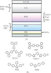
The device configurations of the multilayer UV OLEDs are shown in Fig. 1(a). The CBP and TCTA were each used as HTL. The OXD-7, TAZ, and PBD were each used as EML. The PBD and Alq3 each were used as ETL. The molecular structures of some of the HTL and EML materials used are shown in Fig. 1(b).
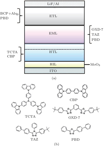 | Fig. 1. (a) Device configurations of the multilayer UV OLEDs. (b) Molecular structures of TCTA, CBP, OXD-7, TAZ, and PBD. |
The current density– voltage and EL spectra of the devices were measured simultaneously by a testing setup comprising of a Keithley 2400 Source Meter and an Ocean Optics USB 4000. The PL spectra of thin film were measured by a Hitachi F4500 fluorescence spectrophotometer. The optical power was measured by a Newport Optical Power Meter 1830-C. All of the measurements were carried out at room temperature under ambient conditions.
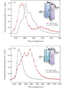
The normalized EL spectra of devices A and B are shown in Figs. 2(a) and 2(b), respectively. The PL spectra of CBP and TCTA are also incorporated in the figure for comparison. The emission of OXD-7 with a peak wavelength of 384 nm is observed in device A, indicating that holes partially overcome the energy barrier and enter into the EML. For the shoulder emission of 485 nm, it is considered to be due to the fact that the recombination of an electron– hole pair building an excited state extended on two neighboring molecules of different chemical natures, which are bonded as a result of the Coulomb interaction.[22] We call it exciplex in the following discussion. The difference in ionization potentials between the two adjacent materials constituting the heterojunction (HTL and EML) is the prime factor governing exciplex formation. Here, the exciplex emission of 485 nm results from the recombination of holes and electrons accumulated at the interface between OXD-7 and CBP. The energy barriers of the lowest unoccupied molecular orbital (LUMO) level and HOMO level are 0.4 eV and 0.5 eV, respectively, as shown in the inset in Fig. 2(a). The redshift is an essential feature of exciplex radiation since the electron– hole pair bound in an exciplex possesses low energy in comparison with an electron– hole pair bound in an exciton.
 | Fig. 2. (a) Normalized PL spectrum of neat CBP in a solid-state film and the normalized EL spectrum of device A. (b) Normalized PL spectrum of neat TCTA in a solid-state film and the normalized EL spectrum of device B. Insets in panels (a) and (b) show the schematic energy level diagrams of devices A and B, respectively. |
In comparison with device A, device B possesses a high energy barrier (0.8 eV) for holes injecting into the EML as shown in the inset in Fig. 2(b). The accumulated holes at the HTL/EML interface lead to the exciplex emission which occupies most of the EL spectrum, as shown in Fig. 2(b). The shoulder emission of 439 nm and peak emission of 488 nm mainly results from direct cross recombination of electrons– holes at the interface between TCTA and OXD-7. Additionally, the negligible electron injection barrier from the EML to HTL induces the emission from TCTA. Consequently, the EL spectrum of device B shows a TCTA shoulder emission at 388 nm from the eigen-excitation of TCTA, which is consistent with the PL emission peak of TCTA. Generally, the fraction of radiative exciplex recombination is a major part, and the formation of exciplex lowers the efficiency of OLED.
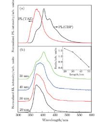
The normalized EL spectra in this subsection are shown in Figs. 3(a) and 3(b). The insets in Figs. 3(a) and 3(b) show the schematic energy level diagrams of devices C and D, respectively. For device A, the emission peak is located at 384 nm with a shoulder emission of 485 nm, as shown in Fig. 2(a). The PL emission from the neat TAZ film (20-nm thick) is examined as shown in Fig. 3(a). For device C, the EL peak of 376 nm is almost identical to the PL peak of TAZ. In device C, the hole-injection barrier at the interface of CBP/TAZ is 0.3 eV less than that of CBP/OXD-7. Consequently, the low energy barrier in device C is more convenient for holes to cross CBP and enter into TAZ. In addition, CBP has a shallower LUMO level than TAZ (0.3 eV, see Fig. 3(a)), which confines the electrons in the EML, thus preventing emission from the HTL. The maximum external quantum efficiency (EQE) of device C is 1.2% and the maximum optical radiation density is 0.11 mW/cm2. It is demonstrated that an energy barrier of over 0.3 eV between EML and adjacent transport layer facilitates the exciplex formation. For device D, the emission peak of 406 nm is different from the PL emission of PBD (397 nm), although the PBD has the same HOMO level of 6.2 eV (as compared with TAZ). The fact that the LUMO level (2.4 eV) of PBD is identical to that of CBP allows the electrons to travel freely. Furthermore, the property of extremely high electron mobility in PBD also contributes to this behavior. The recombination process predominantly occurs in CBP. The luminous efficiency is rather low due to the fact that the emitting zone is quite close to the doped region where carrier quenching exists. As discussed above, it is clear that the choices of materials and well aligned energy levels of EML and HTL both play a key role in UV OLEDs. Effective hole injection and electron blocking demonstrate that the electrons– holes recombination occurs in the EML and avoids the formation of exciplex. In addition, for UV-OLED, the low mobility of electron transport material, to a certain extent, balances the hole and the electron due to hard hole injection.
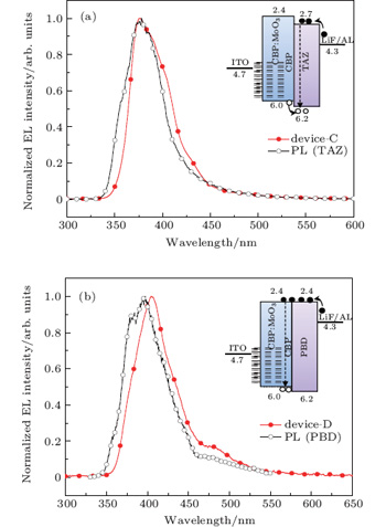 | Fig. 3. (a) Normalized EL spectrum of device C and the PL spectrum of neat TAZ in a solid-state film. (b) Normalized EL spectrum of device D and the PL spectrum of neat PBD in a solid-state film. The insets in panels (a) and (b) show the schematic energy level diagrams of devices C and D, respectively. |
The normalized PL and EL spectra of devices C, E, F, and G are shown in Fig. 4. It is clear that the emission peaks of devices C, E, F, and G are 376 nm, 376 nm, 389 nm, and 406 nm, respectively. The EL emissions of devices C and E predominantly result from eigen-excitation of TAZ. However, the shoulder emission of 406 nm is observed and is gradually predominant with the increasing thickness of TAZ. Moreover, the ratio of the EL intensity of TAZ (λ = 376 nm) to that of CBP (λ = 406 nm) shows a monotonic decrease, as shown in the inset in Fig. 4. With the thickness increases to 40 nm, the ratio approaches to 1. We suppose that the emission regions occur both in TAZ and CBP due to the rather high concentration of injected electrons from the cathode. When the thickness of TAZ increases to 50 nm, the ratio reaches 0.643. As the thickness of TAZ increases, more electrons flow into the CBP layer. The eigen-excitation of TAZ (λ = 376 nm) gradually decreases while that of CBP (λ = 406 nm) gradually increases.
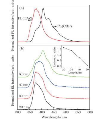 | Fig. 4. (a) Normalized PL spectra of CBP and TAZ (solid-state film), and (b) normalized EL spectra of device C, E, F, and G. The inset shows the ratio of EL intensity of TAZ (λ = 376 nm) to that of CBP (λ = 406 nm) as a function of TAZ thickness. |
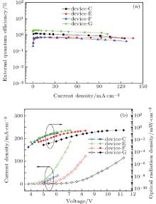
Figure 5(a) shows the dependences of EQE on current density for the UV OLEDs based on TAZ. Figure 5(b) shows the radiant emittance (R)– current density (J)– voltage (V) curves. Additionally, the values of maximum EQE, maximum R of devices C, E, F, and G are listed in Table 1. Device C shows a maximum EQE of 1.2% achieved at J = 3.5 mA/cm2. This efficiency is the highest in the reported values for UV OLEDs with peak emission below 380 nm. Device E shows much higher radiant emittances, owing to its higher current density. These completely different device behaviors, including different EL spectra, R– J– V characteristics, and EQEs for TAZ-based UV OLED, indicate that the devices behave in different emission regions according to the change in the EML thickness and they generate tunable UV emissions from 376 nm to 406 nm.
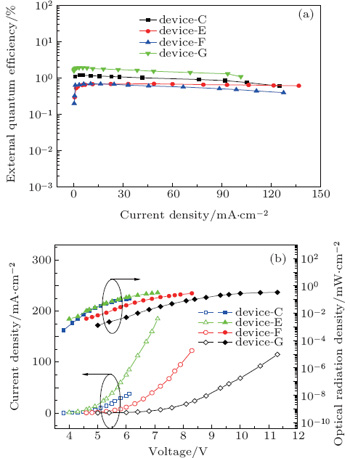 | Fig. 5. (a) Variations of EQE with current density of these UV OLEDs. (b) R– J– V characteristics of UV OLEDs. |
| Table 1. UV-OLED key parameters of devices C, E, F, and G. |
Figure 6 shows the normalized EL spectra of devices H, I, J, and K with various EMLs and ETLs. It can be observed that the EL peaks of devices H and I are at 406 nm, which results from the eigen-excitation of CBP. However, the emission peak of devices J is situated at 391 nm, while that of device K is located at 404 nm. These phenomena reveal that OXD-7 functions as electron transport in devices H and I. The incorporating of the ETL increases the electron concentration. As a result, the emission region is located in CBP and at the interface of CBP/OXD-7, which produces the exciplex emission. For devices J and K, although TAZ behaves as weaker electron migration than OXD-7, the increase of TAZ thickness results in increased electron concentration, which contributes to the emission zone closing to CBP. In addition, the comparison of spectrum between devices J and K shows that the recombination region of device K is more probably close to CBP than that of device J as a result of low electron mobility of Alq3 (weaker than that of PBD). Thus, the emission intensity of 406 nm is much stronger than that of 375 nm in device K. For device J, the peak emission of 391 nm is a mixture of those of both CBP and TAZ. Figure 6(b) also demonstrates that device J displays an additional longer-wavelength emission peak at around 522 nm, which is consistent with the PL spectrum of neat Alq3 in a solid-state film. The absorption of Alq3 near 406 nm does not occur for device H, but the absorption of Alq3 for 391 nm occurs for device J. The experiment with a thin BCP, hole blocking sublayer, inserted into Alq3 layer already excludes the hypothesis that the leaked holes enter into Alq3. It is well demonstrated that, although both 391 nm and 406 nm are within the range of Alq3 absorption spectrum, the absorption of thin film (Alq3) occurs only when it meets the requirement for energy in the device.
 | Fig. 6. (a) Normalized EL spectra of devices H and I. (b) Normalized EL spectra of the devices J and K, and the PL spectrum of neat Alq3 in a solid-state film. The insets in panels (a) and (b) show the schematic energy level diagrams of devices H and J respectively. |
Electronic processes are responsible for charge transporting and EL characteristics in multilayer UV-OLEDs, which are quite sensitive to the properties of organic heterojunctions. In particular, the energy barrier height affects the way electrons and holes meet at heterojunction (exciplexes or excitons) and the probability of photon creation. Although MoO3-doped HTL can effectively provide numerous holes, the high energy barrier of over 0.3 eV located at the interface between EML and adjacent organic layers is conducive to the exciplex formation. It is concluded that appropriate energy level alignment in multilayer UV OLED is imperative to prevent any undesired emission from other layers or interfaces. Finally, it is found that the UV emission can excite low-energy organic function layers and produce PL emission.
| 1 |
|
| 2 |
|
| 3 |
|
| 4 |
|
| 5 |
|
| 6 |
|
| 7 |
|
| 8 |
|
| 9 |
|
| 10 |
|
| 11 |
|
| 12 |
|
| 13 |
|
| 14 |
|
| 15 |
|
| 16 |
|
| 17 |
|
| 18 |
|
| 19 |
|
| 20 |
|
| 21 |
|
| 22 |
|