
Optimal oxide-aperture for improving the power conversion efficiency of VCSEL arrays*
[Wang Wen-Juan, Li Chong, Zhou Hong-Yi, Wu Hua, Luan Xin-Xin, Shi Lei, Guo Xia† ]
]
]
|
|


Corresponding author. E-mail: guo@bjut.edu.cn
Project supported by the National Natural Science Foundation of China (Grant Nos. 61222501 and 61335004) and the Specialized Research Fund for the Doctoral Program of Higher Education of China (Grant No. 20111103110019)
The maximum power conversion efficiencies of the top-emitting, oxide-confined, two-dimensional integrated 2×2 and 4×4 vertical-cavity surface-emitting laser (VCSEL) arrays with the oxide-apertures of 6 μm, 16 μm, 19 μm, 26 μm, 29 μm, 36 μm, 39 μm, and 46 μm are fabricated and characterized, respectively. The maximum power conversion efficiencies increase rapidly with the augment of oxide-aperture at the beginning and then decrease slowly. A maximum value of 27.91% at an oxide-aperture of 18.6 μm is achieved by simulation. The experimental data are well consistent with the simulation results, which are analyzed by utilizing an empirical model.
Vertical-cavity surface-emitting lasers (VCSELs) have been widely used in optical interconnection, optical communications, high-speed data transmission, and many other applications, [1– 3] due to their advantages in terms of low power dissipation, low threshold, high efficiency, high speed modulation, cost-effective, etc.[4, 5] High-power VCSEL arrays are attractive for optically pumping solid-state and fiber lasers. Due to the low round-trip gain of VCSEL, increasing the aperture diameter of each element in the arrays, even to several hundreds of microns, is widely regarded as an effective way to achieve high optical output power. However, the carrier distribution, active gain, and refractive index become non-uniform with the increase of the aperture, which is mainly determined by the spatial hole-burning effect originating from lateral series resistance.[6– 8] Hence, the power conversion efficiency decreases, which is a significant performance in the application of VCSEL arrays. A recent report has shown that the maximum power conversion efficiency of 4× 4 VCSEL arrays with 200-μ m aperture is only about 17.8%.[9] This is difficult to use in practical applications because the power supply must be very high due to the low power conversion efficiency. Seurin et al.[10] found that the maximum power conversion efficiency (MPCE) of the single VCSEL increases quickly with the augment of aperture, it reaches its maximum value at the beginning and then decreases slowly. The MPCE of 50% with an aperture of 10 μ m is achieved for the individual VCSEL. As evidenced by their experimental results, Hofmann et al.[11] demonstrated that the MPCE followed a similar tendency and obtained a maximum value about 22% at a 10-μ m aperture. However, the tendency of MPCE for VCSEL arrays has not yet been analyzed in theory or verified in experiment. Therefore, it is important to systematically understand the relationship between the power conversion efficiency and the aperture of VCSEL array.
In this paper, we investigate the relationship of the power conversion efficiency with the oxide aperture by the top-emitting 2× 2-nm and 4× 4 850-nm VCSEL arrays. Both theoretical analysis and experimental measurement indicate that there exists an optimal oxide aperture for VCSEL arrays to obtain maximum power conversion efficiency. Our study puts forward an insight into the optimization of the VCSEL array design for improving the power conversion efficiency.
The reported VCSEL arrays are fabricated from a metal organic vapor phase epitaxy grown AlGaAs structure on an n-type GaAs substrate. The bottom n-type mirror below the active region consists of 34.5 pairs of Si-doped Al0.9Ga0.1As/Al0.12Ga0.88As distributed Bragg reflectors (DBRs) for high optical reflectivity. The un-doped active region contains three GaAs quantum wells that are centered on the anti-node of the optical standing wave within the one-wavelength cavity, with its photoluminescence peak at 835 nm. The top p-type mirror above the active region consists of 20.5 pairs of C-doped Al0.12Ga0.88As/Al0.9Ga0.1As DBRs, each of which has an Al fraction similar to the bottom n-DBR. Graded interfaces and dopings are used on the top and bottom DBR layer to reduce the differential resistance and maintain low free carrier absorption loss. A single low-index quarter-wavelength Al0.98Ga0.02As oxidization layer in the p-type mirror adjacent to the active region is employed to form an oxide aperture for current and later optical confinement. After that, a highly doped 25-nm GaAs Ohmic contact layer is formed on the top of the epitaxial wafer. The operation wavelength of this structure is designed to be 850 nm.
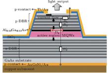
The top-emitting, oxide-confined 2× 2 and 4× 4 850-nm VCSEL arrays are fabricated through a series of processing steps, including mesa etching, wet oxidation, and contact formation, and its schematic cross section is presented in Fig. 1. The fabrication of the VCSEL arrays is described as follows. To form about 3-μ m height cylindrical mesa for exposing the oxidation layer (Al0.98Ga0.02As), the sample was soaked for 9 min in a CH3OH:H3PO4:H2O2 solution with 3:1:1 volume ratio in ice– water mixture, by using 200-nm SiO2 as the etching mask. After that, the Al0.98Ga0.02As oxide-confined layer was selectively wet-oxidized in a high humidity furnace at 400 ° C with a 90-° C water bath and 1-L/min N2 flow in order to form the current oxide-aperture and provide lateral current confinement. The oxide-apertures of VCSEL arrays are 6 μ m, 16 μ m, 19 μ m, 26 μ m, 29 μ m, 36 μ m, 39 μ m, and 46 μ m, respectively. Before evaporating the 15-nm/300-nm Ti/Au p-type annular contact, the surface is passivated by depositing 400-nm SiO2 to electrically insulate all the mesa sidewalls from the p-contact. To minimize absorption losses and resistance series on substrate, the substrate was thinned to around 120 μ m. Then, the evaporation of the 50 nm/300 nm AuGeNi/Au n-type bottom contact and a subsequent annealing process are carried out. Thus, the processing is completed.
The cleaved chips of arrays are attached to the copper subcarriers with indium coating for electrical supply and thermal dissipation. A schematic diagram of individual VCSEL in arrays is shown in Fig. 1. The spacing between the neighboring elements is 50 μ m, which reduces the thermal crosstalk.
 | Fig. 1. Schematic cross-sectional view of the selectively oxidized-confined top-emitting VCSEL, where Da is the oxide-aperture diameter, RL the lateral resistance, RV and   |
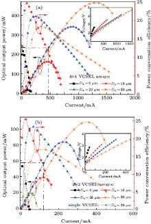
The typical optical output powers and the current– voltage (I– V) performances of 4× 4 VCSEL arrays with the apertures of 6 μ m, 19 μ m, 29 μ m, and 39 μ m are presented in Fig. 2(a), respectively, under the pulsed operation with a pulse width of 50 μ s and a repetition rate of 100 Hz at room temperature. As the current injection increases, the optical output power increases to the thermal rollover point that is induced by carrier leakage and joule heat caused by series resistance.[14, 15] The threshold currents of the arrays exhibit 0.91 mA, 15.09 mA, 50.93 mA, and 88.05 mA, respectively. Maximum optical output powers of 16.45 mW, 161.97 mW, 341.03 mW, and 464.23 mW are obtained. The slopes of I− V curves, which represent the differential resistances, decrease with the increase of oxide-aperture, owing to the reduced lateral resistance through the oxide-aperture to the active region.[16] The differential resistances are 6.54 Ω , 3.08 Ω , 2.73 Ω , and 2.18 Ω , respectively.
The power conversion efficiency of VCSEL arrays, which also is presented in Fig. 2(a), is calculated from

where Pex is the optical output power, Pin is the electrical output power, I is the driven current, V is the applied voltage, hν is the photon energy, q is the electronic charge, η e is the external differential quantum efficiency, Ith is the threshold current, Rs is the differential resistance (dV / dI), V0 the turn-on voltage (zero-current intercept), and the measured value is 1.68 V. The values of η e of around 23.16%, 51.13%, 56.95%, and 52.30% are calculated from η e = [(Pex − Pt)/hν ]/[(I − Ith)/q], [4] where Pt is the optical output power at the threshold current. The values of MPCE are 12.33%, 27.30%, 22.12%, and 18.34%, respectively. The optical output power, the current– voltage (I– V) curve, and power conversion efficiency of 2× 2 VCSEL arrays with the apertures of 6 μ m, 19 μ m, 29 μ m, and 39 μ m are shown in Fig. 2(b), respectively. Figures 2(a) and 2(b) show that, as the oxide-aperture increases, the values of the MPCE first increase due to the decrease of differential resistance, and then decrease for both 2× 2 and 4× 4 VCSEL arrays.
The single VCSEL emitter with a 29-μ m oxide-aperture has an output power of 14.34 mW at 30-mA bias current from Fig. 2(b). This means that the theoretically expected output power of an array of 4 or 16 elements biased at 4 × 30 mA= 120 mA or 16 × 30 mA= 480 mA is 4 × 14.34 mW= 57.36 mW or 16 × 14.34 mW= 229.44 mW; the two values are close to the ideal values considering that there is no heat generation inside the VCSELs. This result emphasizes that there is very mild thermal crosstalk among elements and these VCSEL arrays have the potential to be scaled up to achieve higher powers, so the thermal problem in our study can be ignored.
 | Fig. 2. Plots of optical output power, power conversion efficiency, and voltage in insets versus current with the values of oxide-aperture Da of 6 μ m, 19 μ m, 29 μ m, and 39 μ m for (a) 4× 4 VCSEL arrays and (b) 2× 2 VCSEL arrays. The dash– dot lines represent the output powers of 14.34 mW, 57.30 mW, and 235.90 mW for the single VCSEL emitter, the 2× 2 VCSEL and the 4× 4 VCSEL arrays with 29-μ m oxide-apertures, at 30 mA, 120 mA, and 480 mA, respectively. |
The power conversion efficiency of VCSEL arrays can be improved by enhancing the external differential quantum efficiency, and reducing the threshold current and the differential resistance. But these three limiting factors also influence and restrict each other. As the oxide-aperture increases, the following expected trend can appear: a decrease in differential resistance, an increase in threshold current, and an increase in external differential quantum efficiency. Therefore, the MPCE is affected synthetically by differential resistance, threshold current, and external differential quantum efficiency. To better understand the various physical processes, it is significant to further analyze the interaction of the three factors.
The MPCE is a function of external differential quantum efficiency, threshold current, and differential resistance, and according to dη PCE/dI = 0, [4, 10, 17] the analytical expression can be expressed as
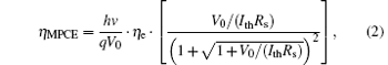
in which Rs is the sum of the series-connected lateral resistance RL and the vertical resistance RV of p-DBR, which is a function of aperture size Da, because the 

where ρ L and ρ V are the lateral and vertical characteristic resistivity, respectively, n is the element number in the array. The lateral resistance RL = ρ L/(π Da) represents the lateral and contact resistance, which derives from the current or carrier spreading through contact, and it is inversely proportional to the oxide-aperture perimeter. The vertical resistance RV = ρ V/[π (Da/2)2] relates to uniform vertical current flow or carriers through the oxide-aperture, meanwhile the resistance is inversely proportional to the oxide-aperture area and its resistivity ρ V essentially represents the vertical resistivity of the p-DBR.[4] The analytical expressions of the external differential quantum efficiency and the threshold current as a function of aperture size can be, respectively, represented as[4, 13]


where I0 is the characteristic spreading current, D0 the characteristic spreading distance, J∞ and η ∞ are the threshold current density and the external differential quantum efficiency under a uniform current distribution, respectively, which depend only on the intrinsic structure of the device.
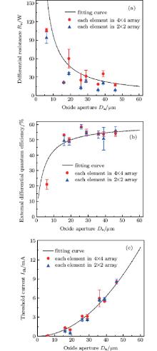
Figures 3(a)– 3(c) show the experiment data extracted from Fig. 2 the differential resistance of each element in arrays, the external differential quantum efficiency, and the threshold current each as a function of Da. The lines in Fig. 3 show the fitting results according to Eqs. (3)– (5), which demonstrate that the differential resistance decreases as Da increases, the external differential quantum efficiency increases as Da increases, and then reaches a saturation value. Meanwhile, the threshold current always increases quickly as Da increases, due to the increase of the active volume. The characteristic parameters of ρ L, ρ V, J∞ , D0, I0, and η ∞ are extracted and shown in Table 1, by the numerical fitting results according to Eqs. (3)– (5).
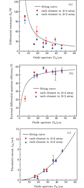 | Fig. 3. Experimental data and the numerical fitting curves of (a) the differential resistance of each element in arrays, (b) the external differential quantum efficiency, and (c) the threshold current versus the oxide-aperture. The data are the measured data and the error bars represent the standard deviation of arrays. |
| Table 1. Calculated and extracted characteristic parameters of VCSEL arrays. |
Figure 4 shows the calculated MPCE curve of VCSEL arrays as a function of aperture size, according to Eq. (2). All of the simulation data are based on the fitting results of Fig. 3. The MPCE increases rapidly as the aperture size increases, which is due to the decrease of the electrical dissipation, [18] and then decreases slowly after it has reached its maximum, which is attributed to the combined interaction of differential resistance, threshold current, and the external differential quantum efficiency. According to our device structure, the maximum MPCE is 27.91% at an 18.6-μ m oxide-aperture. For an aperture size ranging from 15 μ m to 25 μ m, the MPCE could reach 99% of the maximum value. With the increase of the aperture size, the threshold current keeps increasing but the differential resistance and the external differential quantum efficiency have little change, which causes the value of MPCE to decrease gradually to zero[13] according to Eq. (2).
The experimental data, which are calculated according to the measurement results, are also shown in Fig. 4, and its behaviour is approximately consistent with the calculated MCPE curve. The measured maximum values of MPCE are 28.6% and 27.6% with an aperture size of 16-μ m oxide-aperture for 2× 2 and 4× 4 VCSEL arrays, respectively, which are close to the calculated maximum value. The experimental data are slightly lower than the numerical calculation curve, especially for an aperture size above 25 μ m. We believe that there still exists a slight thermal effect among the adjacent elements of arrays which need high current injection.[14, 19]
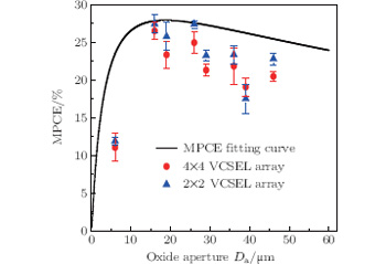 | Fig. 4. The MPCE versus the oxide aperture of the experimental data and the numerical fitting curves of VCSEL arrays, where the data are the measured data and the error bars represent standard deviations of five arrays. |
The deviation between the experimental data and the numerical fitting curve increases as the oxide-aperture augments. In the analysis above, figures 3(a)– 3(c) show the fitting curves of the differential resistance, the external differential quantum efficiency, and the threshold current, each as a function of the oxide-aperture based on Eqs. (3)– (5), when the thermal crosstalk problem among elements is ignored. However, for an actual VCSEL array device, there still exist small errors in the numerical fitting processes of the differential resistance, the external differential quantum efficiency, and the threshold current derived from the crosstalk problem. The deviation accumulation between the experimental data and numerical fitting can ultimately lead to a relatively great influence on the values of MPCE. With the increase of the oxide-aperture, the deviation increases because the increasingly serious crosstalk and the larger oxide-aperture will lead to a non-uniform injection current for the annular electrode.[6, 20]
The relationship between MPCE and the oxide-aperture of VCSEL arrays is analyzed by using an empirical model. The MPCE increases rapidly with the oxide-aperture increase and then decreases slowly after it has reached its maximum, which is attributed to the combined interaction of differential resistance, threshold current, and external differential quantum efficiency. The maximum value of MPCE is 27.91% at 18.6-μ m optimal oxide-aperture and can reach 99% of the maximum value in an aperture size range from 15 μ m to 25 μ m. The experimental data match the theoretical analyses well. The analyses of the various oxide-apertures contributing to the MPCE saturation of the device can provide a guidance for improving the power conversion efficiency.
| 1 |
|
| 2 |
|
| 3 |
|
| 4 |
|
| 5 |
|
| 6 |
|
| 7 |
|
| 8 |
|
| 9 |
|
| 10 |
|
| 11 |
|
| 12 |
|
| 13 |
|
| 14 |
|
| 15 |
|
| 16 |
|
| 17 |
|
| 18 |
|
| 19 |
|
| 20 |
|