

Preparation of graphene on Cu foils by ion implantation with negative carbon clusters*
Cite this Article
Li Hui, Shang Yan-Xia, Zhang Zao-Di, Wang Ze-Song, Zhang Rui, Fu De-Jun. Preparation of graphene on Cu foils by ion implantation with negative carbon clusters* . Chinese Physics B, 2014, 24(1): 018502 
Permissions
Preparation of graphene on Cu foils by ion implantation with negative carbon clusters*
Corresponding author. E-mail: djfu@whu.edu.cn
Project supported by the National Natural Science Foundation of China (Grant Nos. 11105100, 11205116, and 11375135) and the State Key Laboratory of Advanced Welding and Joining, Harbin Institute of Technology, China (Grant No. AWJ-M13-03).
Abstract
We report on few-layer graphene synthesized on Cu foils by ion implantation using negative carbon cluster ions, followed by annealing at 950 °C in vacuum. Raman spectroscopy reveals IG/ I2D values varying from 1.55 to 2.38 depending on energy and dose of the cluster ions, indicating formation of multilayer graphene. The measurements show that the samples with more graphene layers have fewer defects. This is interpreted by graphene growth seeded by the first layers formed via outward diffusion of C from the Cu foil, though nonlinear damage and smoothing effects also play a role. Cluster ion implantation overcomes the solubility limit of carbon in Cu, providing a technique for multilayer graphene synthesis.
Keyword:
85.40.Ry; 68.65.Pq; 78.30.–j; ion implantation; carbon clusters; graphene; copper foil
1. Introduction
Graphene has attracted much interest since it was discovered in 2004.[1] As the first two-dimensional crystalline material, graphene is promising for applications in many fields, such as nanoelectronics, solar cells, and touch panels.[2, 3] For these practical applications, preparation of large-area and high-quality graphene is necessary.[4, 5] Current methods for graphene synthesis include mechanical exfoliation of graphite, pyrolysis of SiC, reduction of graphite oxide, and chemical vapor deposition (CVD).[6– 13] Recently, researchers have prepared few-layer and even single-layer graphene on Ni films and foils by ion implantation.[14– 16] However, no work has been reported on graphene synthesis on Cu by the ion beam technique. In fact, Cu is advantageous over Ni since carbon has much lower solubility in Cu. In this work, we implanted negative Cn clusters into Cu foils to demonstrate the feasibility for graphene synthesis.
2. Results and discussion
The ion implantation was carried out by using C1, C2, and C4 clusters extracted from the Cs sputtering negative ion source of a 1.7 MV tandetron accelerator. The Cu foils with a purity of 99.8% were purchased from Alfa Aesar, with a thickness of 25 μ m. The substrates were annealed and cut into pieces of 10× 10 mm2. Carbon monomers and clusters were implanted at different energies with carbon dosages of 4× 10¹⁵ and 8× 10¹⁵ atoms/cm2, respectively. The implanted samples were annealed in vacuum following the scheme shown in the inset of Fig. 1. Raman spectra were measured on a Horiba-800 Raman microscope in ambient atmosphere. The excitation source was an Ar laser with a wavelength of 488 nm and a power of 10 mW. The baseline from Cu foil was subtracted in order to show clear Raman features.
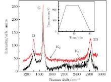
 | Fig. 1. Raman spectra of the graphene samples on Cu foils prepared by cluster ion implantation at 20 kV with monomer C to doses of 4× 10¹⁵ atoms/cm2 and 8× 10¹⁵ atoms/cm2. The inset shows the scheme of the thermal process. |
The first two samples K1 and K2 were made using C1 ions and underwent vacuum annealing. The front sides which C ions impacted directly showed clear Raman features of graphene, while no scattering was detected from the back sides (Fig. 1). It is clear that the thin layers synthesized on the Cu surface are few-layer graphene, with their G and 2D peaks at around 1580 cm− 1 and 2700 cm− 1, respectively.[17, 18]
Table 1 lists the G and 2D peak positions and I2D/IG and IG/ID ratios for Samples K1 and K2 and the FWHM values of the G peaks, which reflect the defect degree of graphene. These values fall in the range of Raman parameters for multilayer graphene.[18, 19] In principle, more carbon atoms implanted into the Cu foil mean more layers of graphene sheets. This rule is well obeyed in the above experiment, since Sample K1 with less C atoms has a smaller IG/I2D value than Sample K2, indicating less layers. Concerning the IG/ID ratios and FWHMs of the G peaks, we find that Sample K2 which possesses more graphene layers has fewer defects, confirming the results reported in Ref. [20].
| Table 1. Raman scattering parameters of graphene samples. |
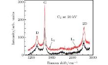
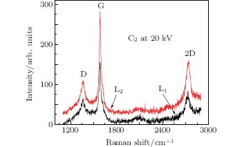
Figures 2 and 3 show Raman spectra of samples (L1 and L2, M1 and M2) prepared by C2 and C4 implantation at 20 keV per cluster with C dosages of 4× 10¹⁵ atoms/cm2 and 8× 10¹⁵ atoms/cm2 followed by annealing under the same scheme. The spectra display clear D, G, and 2D peaks, indicating the formation of graphene. As shown in Table 1, the IG/ID ratios confirm formation of more graphene layers when larger quantity of carbon are implanted in Cu. Similarly, the number of defects in graphene decreases with increasing number of layers.
 | Fig. 2. Raman spectra of graphene on Cu foils prepared by ion implantation with C2 clusters to doses of 4× 10¹⁵ and 8× 10¹⁵ atoms/cm2. The energy is 20 keV per cluster. |
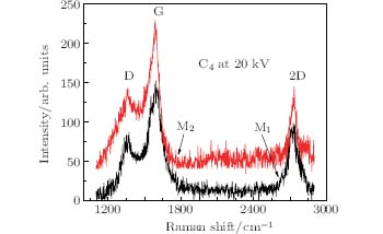 | Fig. 3. Raman spectra of graphene on Cu foils prepared by ion implantation with C4 clusters to doses 4× 10¹⁵ and 8× 10¹⁵ atoms/cm2. The energy is 20 keV per cluster. |
Although the samples were prepared with the same extraction voltage (cluster energy) and carbon dosages, the difference in carbon cluster sizes leads to variation in Raman spectra. The most likely reason is that impact of different clusters has caused different damage in the substrates, and thus different carbon distributions, eventually different graphene sheets.[21, 22] That is, the numbers of graphene layers increase with the carbon doses while the number of defects decreases with the doses, as mentioned above. This explains the change of number of graphene layers and confirms that the layer number can be controlled in the cluster ion beam process.
As to the reason for fewer defects in thicker multilayer graphene, we attribute it to specific growth mechanism of graphene in Cu foils. It is usually difficult to synthesize large-area multilayer graphene films with the CVD method, for instance, due to the self-limiting process caused by the low solubility of carbon in copper.[23, 24] Instead, the graphene samples prepared in this work are mostly multilayers. This suggests that the ion beam process has a different mechanism leading to graphene formation, as schematically shown in Fig. 4. During annealing, implanted carbon atoms close to the substrate surface come out first as the diffusion process starts, and crystallize as graphene under the catalysis of Cu. Then, the C atoms in the depth emerge on the surface, rearrange and bond together as the second graphene layer under the first layer. This process is repeated until the deepest carbon atoms diffuse to the surface. Because of the atomically smooth surface of graphene, [1, 25] the graphene layers formed earlier at the Cu surface will provide a flat plane for latter graphene growth, instead of the Cu substrate with lots of defects. Therefore, more graphene layers tend to have fewer defects.
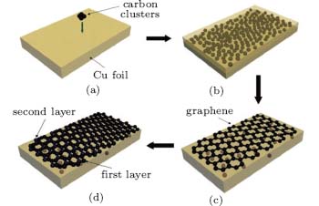 | Fig. 4. Formation mechanism of graphene on a Cu foil by carbon cluster ion implantation followed by annealing and cooling. |
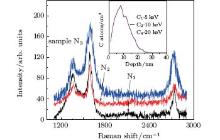
To examine the influence of nonlinear irradiation damage on graphene formation, we prepared a third group of samples, N1, N2, and N3, conducted with 5 kV C1, 10 kV C2, and 20 kV C4, respectively, to a dose of 4× 10¹⁵ atoms/cm2. In this case, the impact energies per carbon atom for the three samples are also identical, equaling 5 kV per atom. According to SRIM simulation for monomer ions (inset of Fig. 5), the implanted carbon atoms from these three clusters should have the same depth distribution in Cu, and thus form the same graphene sheets. However, as shown in Fig. 5 and Table 2, the graphene formed is different from each other, including the number of graphene layers and amount of defects. This demonstrates significant influence of nonlinear damage. As shown by Popok et al., [26] larger clusters produce more defects and higher yield of amorphization in the substrate in comparison with monomer ions if their Eat (energy per atom) values are the same. These defects and amorphization impede the diffusion of C atoms during annealing. As a result, fewer C atoms can diffuse to the substrate surface to coalesce and form graphene. As for the reduced amount of defects in graphene at larger clusters, we believe it is due to smoothing and amorphization effect caused by the clusters.[21, 26] In particular, the smoothing effect reduces the surface hills and slopes, providing a flatter surface for the growth of graphene.[25]
 | Fig. 5. Raman spectra of graphene prepared by ion implantation with C1 at 5 kV, C2 at 10 kV, and C4 at 20 kV, which means they have the same energy per atom, 5 keV per atom. The carbon doses are also the same: 4× 10¹⁵ atoms/cm2. The inset shows SRIM simulation of depth profile of C atoms in Cu. The clusters C15 keV, C210 keV, and C420 keV have identical C distribution according to the simulation. |
| Table 2. Raman scattering parameters of graphene. |
3. Conclusion
In conclusion, we have fabricated multilayer graphene on Cu foils by ion implantation using negative carbon monomer and Cn cluster ions at room temperature. By changing the cluster size and energy, different graphene films were synthesized. The solubility limitation of carbon in Cu is lifted by the cluster ion implantation in comparison with other methods. The number of graphene sheets and amount of defect have been explained by seeded growth, taking account of nonlinear damaging and smoothing effects induced by the cluster ion process.
Reference
| 1 |
|
| 2 |
|
| 3 |
|
| 4 |
|
| 5 |
|
| 6 |
|
| 7 |
|
| 8 |
|
| 9 |
|
| 10 |
|
| 11 |
|
| 12 |
|
| 13 |
|
| 14 |
|
| 15 |
|
| 16 |
|
| 17 |
|
| 18 |
|
| 19 |
|
| 20 |
|
| 21 |
|
| 22 |
|
| 23 |
|
| 24 |
|
| 25 |
|
| 26 |
|