

High-crystalline GaSb epitaxial films grown on GaAs(001) substrates by low-pressure metal–organic chemical vapor deposition*
Cite this Article
Wang Lian-Kai, Liu Ren-Jun, Lü You, Yang Hao-Yu, Li Guo-Xing, Zhang Yuan-Tao, Zhang Bao-Lin. High-crystalline GaSb epitaxial films grown on GaAs(001) substrates by low-pressure metal–organic chemical vapor deposition* . Chinese Physics B, 2014, 24(1): 018102 
Permissions
High-crystalline GaSb epitaxial films grown on GaAs(001) substrates by low-pressure metal–organic chemical vapor deposition*
Corresponding author. E-mail: zhangyt@jlu.edu.cn
Corresponding author. E-mail: zbl@jlu.edu.cn
Project supported by the National Natural Science Foundation of China (Grant No. 61076010) and the International Science and Technology Cooperation Program of Science and Technology Bureau of Changchun, China (Grant No. 12ZX68).
Abstract
Orthogonal experiments of GaSb films growth on GaAs(001) substrates have been designed and performed by using a low-pressure metal–organic chemical vapor deposition (LP-MOCVD) system. The crystallinities and microstructures of the produced films were comparatively analyzed to achieve the optimum growth parameters. It was demonstrated that the optimized GaSb thin film has a narrow full width at half maximum (358 arc sec) of the (004) ω-rocking curve, and a smooth surface with a low root-mean-square roughness of about 6 nm, which is typical in the case of the heteroepitaxial single-crystal films. In addition, we studied the effects of layer thickness of GaSb thin film on the density of dislocations by Raman spectra. It is believed that our research can provide valuable information for the fabrication of high-crystalline GaSb films and can promote the integration probability of mid-infrared devices fabricated on mainstream performance electronic devices.
Keyword:
81.15.Gh; 81.15.Kk; 81.05.Ea; 81.10.Aj; crystal growth; metal–organic chemical vapor deposition; thin films
1. Introduction
In recent years, the research on antimonide semiconductors has made much progress, such as the applications in a monolithic microwave integrated circuit (MMIC), [1] infrared focal plane array detectors, [2] infrared lasers, [3] quantum-cascade lasers, [4] quantum-dot lasers, [5] quantum-well lasers, [6] thermoelectric devices, [7] thermophotovoltaic devices, [8, 9] and resonant tunneling diodes.[10– 14]
Both GaSb and GaAs are III– V semiconductors, which have the same crystal structure and a type-II band alignment can be developed by the GaSb/GaAs heterostructure. The spatial separation of electrons and holes in type-II structures results in long exciton lifetimes.[15] Therefore, GaSb/GaAs heterostructures are very promising for integrated optoelectronics applications.
However, the far-ranging practical applications of GaSb thin films in reliable functional devices have been delayed because of the difficulties in acquiring high-quality epitaxial layers. The main problem in the growth of GaSb epitaxial layers on GaAs substrates is the relatively large lattice mismatch (∼ 8%) that leads to a high threading dislocation density.[16] In addition, different from other group III– V semiconductors, antimonide such as GaSb comprises two metallic elements exclusively. The metallicity of Sb results in a low surface mobility of adatoms, which usually makes the surface of the GaSb epitaxial layer rough. It is widely believed that both surface plainness and crystalline quality are crucial for fabricating antimonide devices on GaAs substrates, however, only a few results on crystalline quality of GaSb films growth on GaAs substrates by MOCVD technology have been reported.[16, 17]
In this paper, orthogonal experiments of GaSb films grown on GaAs substrates have been designed; the crystallinity and microstructure characteristics of the films have been comparatively analyzed to achieve the optimum growth parameters.
2. Experiments
According to the statistics theory of orthogonal experiments designed by Taguchi Gen’ ichi, [18] 16 samples of GaSb films grown on GaAs substrates have been designed. Here, the terms S1– S16 mean sample 1– sample 16, respectively. The growth temperature, growth pressure, and vapor V/III ratio were used as three factors, and each factor contains four levels, as shown in Table 1. The crystalline crystal index (CQI) in Table 1 will be introduced in the next part. After that, a new sample was used to verify the optimal growth conditions inferred from the orthogonal experiments. The GaSb films were grown on semi-insulating GaAs(001) substrates (Epi-ready) by the LP-MOCVD system. The growth time for GaSb films was set as 30 min.
| Table 1. The design of orthogonal experiments of GaSb films growth on GaAs substrates and the CQIs (n/a means the sample did not acquire the diffraction peak by x-ray diffraction measurements. |
3. Results and discussion
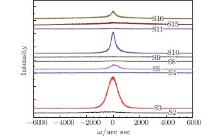
In order to quantifying the crystallinity of GaSb epitaxial layers, ω -rocking curves were measured using the FWHM values of rocking curves. As shown in Fig. 1, a significant change can be observed in ten samples. The abnormal phenomena for samples 2, 4, 8, 9, 11, and 15 probably result from the ultrathin thickness of GaSb films.
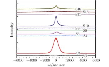 | Fig. 1. X-ray rocking curve patterns of samples S2, S3, S4, S5, S8, S9, S10, S11, S15, and S16. |
The crystalline crystal index (CQI), which means the natural logarithm of FWHM of XRD ω -rocking curves (CQI = ln [FWHM(ω )]), can be used to evaluate the crystalline quality of GaSb epitaxial films in this work. The detailed CQIs of the orthogonal experiments were summarized in Table 1.
Table 2 presents the average results of CQIs for different growth parameters. Note that the CQIs of the samples that did not acquire diffraction peaks by x-ray diffraction (XRD) measurements were set at 10. Then the average results as a function of the growth parameters were calculated. In addition, the differences between the maximum and the minimum values R are given for individual growth parameters.
| Table 2. Average results of CQIs for different growth parameters. R refers to the differ, ence between maximum and minimum values for an individual growth parameter. |
From the obtained results shown above, a relationship can be inferred as RGrowth temperature > RGrowth pressure > RV/III at the given growth conditions. In other words, the dependence of GaSb film crystalline quality on the growth temperature is stronger than that on the growth pressure and V/III ratio. It is therefore inferred that the best growth parameters for high-crystalline GaSb epitaxial film are 550 ° C, 90 mbar, and a V/III of 3.
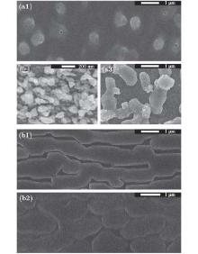
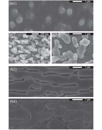
Figure 2 shows the typical morphologies of GaSb products prepared at low and high temperatures. From the figure, we can clearly observe that the surfaces of the GaSb samples grown at a low temperature (Figs. 2(a1)– 2(a3)) have a higher surface coverage. This is because a lower migration length of the atoms results in a connection forming between islands. The sintered type is the main ripening type at a low temperature. By contrast, a higher temperature (Figs. 2(b1)– 2(b4)) leads to a higher level ripening and Ostwald-ripening.[19] Therefore, the films tend to come apart and form big islands.
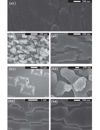 | Fig. 2. Comparison of SEM images of GaSb films fabricated at a low temperature of 500 ° C for S11 (a1), S2 (a2), and S8 (a3) and at a high temperature of 600 ° C for S6 (b1), S4 (b2), S9 (b3), S15 (b4), respectively. |
The GaSb edges of the samples grown at lower pressure are oriented as shown in Figs. 3(a1) and 3(a2). However, the GaSb edges orientation of the samples decrease with growth pressure increasing, as shown in Figs. 3(b1)– 3(b3). The reason is that the mean free path of atoms is longer at the low pressure, which results in not only the adsorption and the deposition of the Ga and Sb atoms, but also that the repinnings between the islands are affected slightly by other atoms.
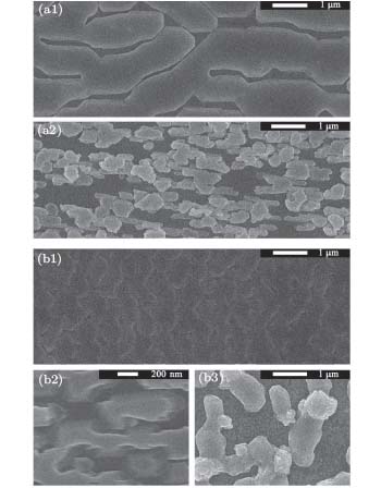 | Fig. 3. Comparison of scanning electron microscope (SEM) images of GaSb films fabricated at a low growth pressure of 30 mbar for S9 (a1), S5 (a2) and at a high growth pressure of 90 mbar for S16 (b1), S8 (b2), and S4 (b3). |
As shown in Fig. 4, a higher portion of Ga atoms led to the formation of film morphologies (Figs. 4(b1) and 4(b2)), and at a low V/III ratio, the produced samples feature islands morphology (Figs. 4(a1)– 4(a3)). Although the migration length of Ga atoms is longer than that of Sb atoms, more Sb atoms can reduce migration length of Ga atoms. Hence, a higher V/III ratio could improve the plainness of GaSb layers, as shown in Figs. 4(b1) and 4(b2). The reason is that the migration length of Ga atoms on GaAs substrate is higher than that of Sb atoms. Thus the small undulation of Ga atom concentration could result in the gathering of adatoms.
 | Fig. 4. Comparison of SEM images of GaSb films fabricated at a low V/III ratio of 0.5 (S3 (a1); S2 (a2); S4 (a3)) and a high V/III ratio of 5 (S15 (b1); S16 (b2)). |
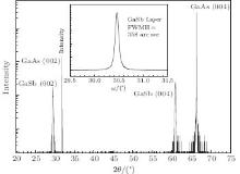
Based on the above results and discussion, a better GaSb epitaxial film with a thickness of 0.7 μ m was obtained as the growth parameters were set at 550 ° C, 90 mbar, and a V/III of 3. Figure 5 shows the typical XRD 2θ scan patterns of the GaSb sample. As expected, diffractions from GaSb (002) and (004) planes were observed, and no other peaks were detected except for the phases from the GaAs substrate. This confirms that the GaSb epitaxial film is highly oriented with its crystallographic c-axis perpendicular to the GaAs substrate and a specified epitaxial relationship was established between the GaSb films and the underlying substrates. Meanwhile, ω -rocking curve measurements of the produced GaSb sample were also performed to check the degree of alignment to the substrate is normal. As shown in the inset in Fig. 5, the FWHM value of GaSb (004) diffraction peak is only 358 arc sec, positively indicating the well-oriented crystallites in GaSb epitaxial film.
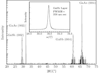 | Fig. 5. XRD 2θ scan pattern of the GaSb epitaxial film grown on GaAs substrate. The inset shows the ω -rocking curve of the GaSb (004) reflection. |
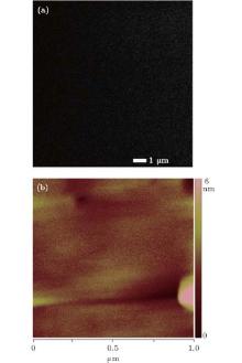
The GaSb epitaxial film presents a smooth surface, as shown in Fig. 6(a), and no obvious grain boundary can be found in the top-view SEM image. The atomic force microscope (AFM) image (Fig. 6(b)) shows that the sample has a relatively small surface roughness of ∼ 6 nm within a scan area of 1 μ m × 1 μ m, which is typical in the case of heteroepitaxial GaSb single-crystal films on GaAs substrates.
 | Fig. 6. (a) SEM and (b) AFM images of GaSb film grown on GaAs substrate. |
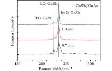
Figure 7 shows the comparative RT Raman spectra of two GaSb/GaAs (001) samples and a bulk GaSb. The growth time of GaSb film has been expanded from 30 min to 60 min for comparison. The thicknesses of the two GaSb films are 0.7 μ m and 1.0 μ m respectively. The Raman excitation used a laser with a wavelength of 532 nm and a power of 0.2 mW. The exposure time for all samples was 10 s. The GaSb longitudinal optical (LO) and transverse optical (TO) phonon mode at the center of the Brillioun zone were detected. The peak position shifting is closely related with the strain in the GaSb film. According to Raman selection rules, the LO phonon mode is allowed and TO is forbidden for the (001) orientation of a zincblende crystal. Because the stress in the GaSb films is released, there is a high density of dislocations in the films, which breaks the symmetry and leads to the appearance of forbidden TO modes.[20] With the increase of the film thickness, the density of the dislocations of the GaSb film decreases accordingly.
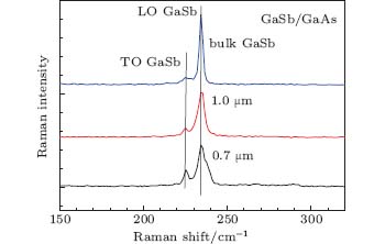 | Fig. 7. Raman spectra from two GaSb/GaAs (001) samples for film thickness of 0.7 μ m, 1.0 μ m, and a bulk GaSb. |
4. Conclusions
Based on the statistical analysis, the following conclusions are obtained: in the process of GaSb film growth on GaAs substrate by means of LP-MOCVD (the scopes of the growth parameter range from 450 ° C to 600 ° C, 30 mbar to 90 mbar, and V/III ratio 0.5 to 5), the dependence of GaSb film crystalline quality on growth temperature is more obvious than that on growth pressure, and that on V/III is minimum. In addition, the combination of parameters of 550 ° C, 90 mbar, and a V/III of 3 is preferable. Through the optimization, a GaSb epitaxial film with a high crystalline quality (358 arc sec of the FWHM of ω -rocking curve) and a low surface roughness of ∼ 6 nm was obtained. The density of dislocations of the optimized GaSb film decreases with the increase of film thickness.
Reference
| 1 |
|
| 2 |
|
| 3 |
|
| 4 |
|
| 5 |
|
| 6 |
|
| 7 |
|
| 8 |
|
| 9 |
|
| 10 |
|
| 11 |
|
| 12 |
|
| 13 |
|
| 14 |
|
| 15 |
|
| 16 |
|
| 17 |
|
| 18 |
|
| 19 |
|
| 20 |
|