


Effect of CoSi2 buffer layer on structure and magnetic properties of Co films grown on Si (001) substrate*
Cite this Article
Hu Bo, He Wei, Ye Jun, Tang Jin, Syed Sheraz Ahmad, Zhang Xiang-Qun, Cheng Zhao-Hua. Effect of CoSi2 buffer layer on structure and magnetic properties of Co films grown on Si (001) substrate* . Chinese Physics B, 2014, 24(1): 017502 
Permissions
Effect of CoSi2 buffer layer on structure and magnetic properties of Co films grown on Si (001) substrate*
Corresponding author. E-mail: zhcheng@aphy.iphy.ac.cn
Project supported by the National Basic Research Program of China (Grant Nos. 2011CB921801 and 2012CB933102), the National Natural Science Foundation of China (Grant Nos. 11374350, 11034004, 11274361, and 11274033), and the Research Fund for the Doctoral Program of Higher Education of China (Grant No. 20131102130005).
Abstract
Buffer layer provides an opportunity to enhance the quality of ultrathin magnetic films. In this paper, Co films with different thickness of CoSi2 buffer layers were grown on Si (001) substrates. In order to investigate morphology, structure, and magnetic properties of films, scanning tunneling microscope (STM), low energy electron diffraction (LEED), high resolution transmission electron microscopy (HRTEM), and surface magneto-optical Kerr effect (SMOKE) were used. The results show that the crystal quality and magnetic anisotropies of the Co films are strongly affected by the thickness of CoSi2 buffer layers. Few CoSi2 monolayers can prevent the interdiffusion of Si substrate and Co film and enhance the Co film quality. Furthermore, the in-plane magnetic anisotropy of Co film with optimal buffer layer shows four-fold symmetry and exhibits the two-jumps of magnetization reversal process, which is the typical phenomenon in cubic (001) films.
Keyword:
75.30.Gw; 75.50.Cc; 75.60.Jk; 75.70.Kw; magnetic anisotropy; CoSi2buffer layers; four-fold symmetry
1. Introduction
The properties of thin magnetic films grown on Si substrate, such as magnetic anisotropy, [1] magnetoresistance, and domain structure have attracted much attention. Especially, Co films have been widely investigated due to their larger magnetic anisotropy constant.[2, 3] Though the hexagonal-close-packed hcp structure is the most stable phase for bulk Co at room temperature, we can use the epitaxial growth way to obtain face-centered-cubic (fcc) phase at room temperature. Unfortunately, Co reacts with Si to form Co1− xSix alloys very easily and also creates a disordered Co/Si interface.[4] Therefore, Co film is hard to grow epitaxially and is always characterized on hcp or polycrystalline phases which all exibit the in-plane uniaxial magnetic anisotropy (UMA).[5] In order to prevent the interdiffusion of Si and Co atoms, some attempts have been performed by inserting a buffer layer of Cu. However, the thickness of this buffer layer is tens even hundreds of nanometer, [3, 6– 8] which is disadvantageous to spin injection in metal/semiconductor system.
In this paper, the CoSi2 layer is chosen as buffer layer, due to its relatively small lattice mismatch (1.23%) with Si substrate and its wide application at the primary contact and narrow gate electrode. Moreover, this buffer layer has no magnetism and no effect on the properties of Co films, which is important in combination of the magnetic materials and semiconductor materials.
In this work, the epitaxial Co films were deposited on Si (001) substrate with various thickness of CoSi2 buffer layer. The magnetic anisotropy of Co films is changed from two fold to four fold, which indicates that the cubic phase is gradually formed. Depending on the field orientation, the hysteresis loops of cubic Co film with one and two steps are observed.
2. Experiment
Experiments were conducted in a molecular-beam epitaxy (MBE) system with a base pressure of 2.0× 10− 10 mbar. After transferred into the ultrahigh vacuum (UHV) chamber, the phosphorus-doped Si (001) substrates were degassed at 600 ° C, followed by a standard direct current flashing process at 1250 ° C.[9, 10] After few seconds of thermal treatment, the atomically flat Si (001)-1× 2 reconstructed surfaces were obtained. In order to avoid the Co– Si intermixing, the first Co film with few monolayers were deposited at room temperature and then annealed for 5 min at 400 ° C to prepare the flat ultrathin C (2× 2) CoSi2 buffer layers. Then, the 10 monolayer (ML) Co films were grown with a deposition rate of 0.75 ML/min. Before taking out the samples from vacuum chamber, another 50 ML of NaCl films were capped to avoid the oxidization of samples. By comparing the ex situ and in situ surface magneto-optical Kerr effect (SMOKE) measurements, the magnetic properties did not change, indicating that the films were not oxidized in air. The surface morphology and structure of the films were characterized by scanning tunneling microscope (STM), low energy electron diffraction (LEED), and high resolution transmission electron microscopy (HRTEM). The in-plane magnetic anisotropy of the films was investigated by ex situ MOKE measurement.
3. Results and discussion
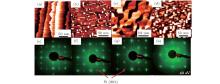
The STM images of CoSi2 buffer layer grown on the Si (001) surface with different thickness from 0 to 3.75 ML are shown in Figs. 1(a)– 1(d). Through the current heating treatment, the atomically flat Si (001) surfaces with sharp step edges were obtained, which is shown in Fig. 1(a). Correspondingly, the Si (001)-(1× 2) reconstructed surface of substrate is demonstrated by LEED measurement. Figures 1(b)– 1(d) illustrate the STM images of the CoSi2 template of 1 ML, 2 ML, and 3.75 ML, and the corresponding CoSi2 C (2× 2) reconstructed LEED patterns are shown in Figs. 1(f)– 1(h), respectively. The epitaxial relationship between CoSi2 and Si (001) is [001]∥ [001] by the LEED analysis. When the cobalt silicide template is very thin, it comprises of some grains owing to the nature property of silicide. The LEED pattern of 1 ML CoSi2 films contains CoSi2 (100)– C (2× 2) phase and Si (001)-(1× 2) phase at the same time, which indicates that the cobalt silicide buffer layer does not cover the entire surface of substrate. As the thickness of CoSi2 increases, the flat and maze cobalt silicide templates are formed and completely cover up the entire substrate at 3.75 ML, which are shown in Figs. 1(b)– 1(d). It also shows the change from the mixture of CoSi2 (001) and Si (001) into pure CoSi2 by the LEED pattern analysis (see Figs. 1(e)– 1(h)). The magnetic properties of buffer layers are also investigated by in situ MOKE. The disappearance of magnetic hysteresis curves indicates that the buffer layer has no magnetism. Those cobalt silicide layers are generally used as a template for preparing ultrathin Co films.
 | Fig. 1. STM and LEED of (a) clean Si(001) substrate and with different thickness of CoSi2 buffer layer: (b) 1 ML, (c) 2 ML, and (d) 3.75 ML. |
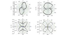
Figure 2 presents the longitudinal MOKE loops of Co films deposited on different thickness of buffer layer. The θ denotes the direction of in-plane external magnetic field with respect to the substrate step (Si [010]). The MOKE hysteresis loops are obtained for all films discussed above (10 ML Co films with different thickness of buffer layer). The angular dependence of coercivity of film without buffer layer as shown in Fig. 2(a) suggests uniaxial magnetic anisotropy. Because the Co reacts with Si and forms disorder Co/Si interface, [6] which results in amorphous or polycrystalline film and makes uniaxial magnetic anisotropy.[1] In Fig. 2(b), the coercivity of Co film with 1 ML CoSi2 at θ = 0° and θ = 90° have the largest (55 Oe) and the smallest coercivity (25 Oe), respectively, indicating that uniaxial magnetic anisotropy still exists in this sample. The complicated symmetry of magnetic anisotropy is observed in sample with 2 ML cobalt silicide template as shown in Fig. 2(c). The coercivity has four maximal multiples of 45° , but is different between θ = 0° and θ = 90° , which can be understood as the superposition of a four-fold and a uniaxial magnetic anisotropy. In samples with 3.75 ML buffer layer, the angular-dependent coercivity exhibits standard four-fold symmetry as displayed in Fig. 2(d). For Co (001) film, magnetocrystalline anisotropy always results in the four-fold magnetic anisotropy. Therefore, the magnetocrystalline anisotropy of cubic phase Co (001) film enhances and dominates in sample with four-fold magnetic anisotropy. The symmetry of magnetic anisotropy changes from UMA to four-fold, which indicates that the quality of cubic phase Co films becomes better as the thickness of CoSi2 buffer layer increases.
 | Fig. 2. Magnetic anisotropy of Co films with different thickness of CoSi2 buffer layer: (a) 0, (b), 1 ML, (c) 2 ML, and (d) 3.75 ML. |
Figure 3(a) shows the schematic configuration of the sample and the coordinate system used in our MOKE measurements. Figure 3(b) shows the LEED pattern of 10 ML Co film deposited on 3.75 ML CoSi2/Si (001) surface. The LEED pattern indicates that four-fold symmetry exists, suggesting a cubic Co (001) film. The epitaxial relationships between the Co (001) film and the Si substrate are as follows: Co(001)[001]/ / Si(001) [001]. The STM image of Co film as shown in Fig.3(c) suggests that it is grown by three-dimensional (3D) islands on Si substrate. The epitaxial growth of film makes elastic energy increase fast, and the constrained film becomes unstable to form three-dimensional islands to strain relief. In our previous work, the same effects of strain at the Fe/FeSi2 interface on the magnetic anisotropy were discussed.[12, 13] Figure 3(d) shows a cross-section HRTEM image of Co film. It can be inferred that the thickness of film is 1.6 nm (about 10 ML) and the quality of crystallization of Co film is good. On the basis of Si single crystal lattice distance, the lattice constant aCo = 3.5 Å is in a good agreement with fcc Co. Moreover, the sharp interface between the substrate and Co film indicates that the buffer layer effectively prevents the interdiffusion of Si and Co film.
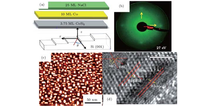 | Fig. 3. (a) Schematic diagram of thin film growth; (b) LEED at 27 eV of Co film with 3.75 ML CoSi2 buffer layer; (c) STM of Co film surface; (d) cross section HRTEM of Co film. |
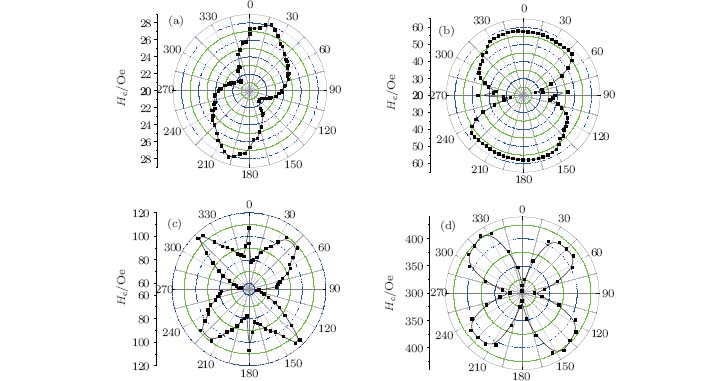
Figure 4 presents the hysteresis loops of Co film with 3.75 ML cobalt silicide template sample along one principal θ = 0° and 45° axis. The θ = 45° axis is along the [110] directions of the Co lattice. The nearly square loop of [110] direction suggests the magnetic easy axis, which can be explained by a negative cubic anisotropy constantK1. This is also reported in other work.[14] The anisotropy strength K1 can be deduced from the formula in the form of
 |
 |
where Eani is the effective anisotropy energy, which is approximately equal to the magnetocrystalline anisotropy energy, [15] and α i is the direction cosine of the magnetization. For the Co (001) plane film, Eani can be simplified into Eq. (2).
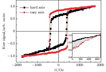 | Fig. 4. Two characteristics hysteresis loops of film with 3.75 ML cobalt silicide template sample along the hard and easy axis. |
The anisotropy energy, which is also approximately equal to the demagnetizing energy, [16] is then calculated (see inset of Fig. 4) according to
 |
Finally, by comparing Eani between θ = 0° and θ = 45° axis, we can obtain the cubic anisotropy constant K1/Ms (K1 = 12.47× 10⁴ J/m3), which is in good agreement with the magnetocrystalline anisotropy of bulk fcc Co (16.5× 10⁴ J/m3).[17]
The easy-axis hysteresis loop of the sample with 3.75 ML CoSi2 buffer layer has a square shape and HC = 420 Oe (see Fig. 4). The HC is smaller than the magnetocrystalline anisotropy effective field of Co film, HC = 2K1/(μ 0Ms) = 1700 Oe, which can be explained by nucleation and propagation of domains in the magnetic reversal process. Near the hard axis, the two-jump loops are already observed and discussed in previous studies on Fe/MgO.[18] In our work, the two-jump loop is not very sharp and can be explained in terms of a combination of coherent rotation and domain wall displacements.
Figure 5(a) shows the two-jump process of hysteresis loop at θ = 81° . According to Cowburn and Zhan’ s results, [18, 19, 20] the two-jump loop appears in a cubic system with small uniaxial anisotropy in the (001) plane of the sample and the ratio r = Ku/K1 < 1. The uniaxial anisotropy is so small in our sample that it has little influence on angular dependence coercivity. The two-jump process can be interpreted in Fig. 5(b). Firstly, the magnetization is away from the field direction θ = 81° by coherent rotation as the positive field decreases. When the field direction is changed and increases up to HC1, magnetization jumps to the near easy axis by domain expansion. The tilting platform between HC1 and HC2 corresponds to coherent-rotation process and the magnetization is away from the easy axis. As negative field increases, the second jump at HC2 results from the magnetization jumping from one easy axis to another one by domain expansion. It undergoes coherent rotation and finally becomes parallel to the direction of the reversed applied field.
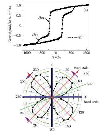 | Fig. 5. (a) Two-jump process of hysteresis loop at θ = 81° . (b) Schematic diagram of magnetization reversal process. |
4. Conclusion
With increasing thickness of CoSi2 buffer layer in Co/Si (001) system, the single cubic phase crystal structure of Co film is gradually formed. The STM and LEED analysis show that the quality of film is strongly affected by the thickness of buffer layer. The optimal thickness of CoSi2 layer needs only few monolayers (3.75 ML). Moreover, the magnetic anisotropy of ultrathin film varies from UMA to four fold by the MOKE analysis. The four-fold symmetry is originated from magnetocrystalline anisotropy of fcc Co. The magnetic hysteresis loop of Co film shows the two-jump magnetization reversal and can be interpreted by coherent rotation and domain wall nucleation.
Reference
| 1 |
|
| 2 |
|
| 3 |
|
| 4 |
|
| 5 |
|
| 6 |
|
| 7 |
|
| 8 |
|
| 9 |
|
| 10 |
|
| 11 |
|
| 12 |
|
| 13 |
|
| 14 |
|
| 15 |
|
| 16 |
|
| 17 |
|
| 18 |
|
| 19 |
|
| 20 |
|