

Different charging behaviors between electrons and holes in Si nanocrystals embedded in SiN x matrix by the influence of near-interface oxide traps*
Cite this Article
Fang Zhong-Hui, Jiang Xiao-Fan, Chen Kun-Ji, Wang Yue-Fei, Li Wei, Xu Jun. Different charging behaviors between electrons and holes in Si nanocrystals embedded in SiN x matrix by the influence of near-interface oxide traps* . Chinese Physics B, 2014, 24(1): 017305 
Permissions
Different charging behaviors between electrons and holes in Si nanocrystals embedded in SiN x matrix by the influence of near-interface oxide traps*
Corresponding author. E-mail: kjchen@nju.edu.cn
Project supported by the National Basic Research Program of China (Grant No. 2010CB934402) and the National Natural Science Foundation of China (Grant No. 11374153).
Abstract
Si-rich silicon nitride films are prepared by plasma-enhanced chemical vapor deposition method, followed by thermal annealing to form the Si nanocrystals (Si-NCs) embedded in SiN x floating gate MOS structures. The capacitance–voltage ( C– V), current–voltage ( I– V), and admittance–voltage ( G– V) measurements are used to investigate the charging characteristics. It is found that the maximum flat band voltage shift (Δ VFB) due to full charged holes (∼ 6.2 V) is much larger than that due to full charged electrons (∼ 1 V). The charging displacement current peaks of electrons and holes can be also observed by the I– V measurements, respectively. From the G– V measurements we find that the hole injection is influenced by the oxide hole traps which are located near the SiO2/Si-substrate interface. Combining the results of C– V and G– V measurements, we find that the hole charging of the Si-NCs occurs via a two-step tunneling mechanism. The evolution of G– V peak originated from oxide traps exhibits the process of hole injection into these defects and transferring to the Si-NCs.
Keyword:
73.63.Bd; 73.40.Qv; 73.90.+f; silicon nanocrystals memory; different charging of electrons and holes; oxide traps; admittance-voltage characteristics
1. Introduction
Three-dimensional confined silicon nanocrystals (Si-NCs) represent a new kind of materials which can be potentially applied for the field of optoelectronics and nanoelectronics, such as light emission devices, single electron transistors, and memory devices.[1– 4] As one of the nonvolatile memory (NVM), Si-NCs floating gate based structures have been widely investigated due to its attractive charge storage characteristics. The main advantage arises from the fact that the charges are stored in Si-NC dots which are isolated from each other. Thus, the data retention characteristics can be remarkably improved. On the other hand, the ultra-thin tunneling oxide layer can be employed to greatly decrease the operating voltage and power cost of a memory cell.
So far, many groups have reported the charge storage characteristics in Si-NCs embedded in SiO2 floating gate metal-oxide-semiconductor (MOS) structures or Si-NCs floating gate MIS structures with an insulating layer of Si3N4, and the C– V and I– V measurements were used to understand the storage mechanism and electronic properties in these structures.[5– 13] However, the charging characteristics of Si-NCs embedded in SiNx floating gate MOS structures have not been reported previously.
In this work, we prepare Si-NCs embedded in SiNx matrix by thermal annealing of the Si-rich silicon nitride film. The formation of Si-NCs is verified by Raman measurements and the cross-sectional high resolution transmission electron microscopy (HRTEM) image. The charging and discharging processes of electrons and holes are systematically studied by C– V, I– V, and G– V measurements. We find that the charging characteristics are different between electrons and holes because the holes injection is influenced by the oxide hole traps. Moreover, we find that the hole charging of the Si-NC dots occurs via a two-step tunneling mechanism. The evolution of G– V peak originated from oxide traps exhibits the process of hole injection into these traps and transferring to the Si-NCs.
2. Experiments
The MOS diode with a sandwiched structure (SiO2/Si-NCs in SiNx/SiO2) was fabricated on a p-type (100) Si substrate with resistivity of 6– 8 Ω · cm. After standard RCA cleaning and the native oxide removing process, a 3-nm thick tunneling SiO2 layer was formed by thermal oxidation at 850 ° C for 15 min in argon-diluted oxygen (10% O2) environment. Then a Si-rich silicon nitride layer (about 4-nm in thickness) was deposited using a mixture gas of SiH4 (2 SCCM) and N2 (40 SCCM) in a plasma enhanced chemical vapor deposition (PECVD) system. The plasma power and growth temperature were fixed at 20 W and 250 ° C, respectively. After that, an about 25-nm thick SiO2 dielectric layer was deposited using a mixture gas of SiH4 (0.5 SCCM) and N2O (50 SCCM), which is served as a blocking layer not only for the confinement of Si-NCs growth during a following thermal treatment but also as an insulating layer to prevent the charge leakage from the gate side. During the thermal treatments, the sample was annealed in N2 ambient at 900 ° C for 30 min and 1100 ° C for 5 min. Finally, aluminum electrodes on the topside and backside were made by the vacuum thermal evaporation, followed by annealing at 400 ° C for 20 min in N2 ambient to improve the contact properties. The diameter of top circular electrode is 200 μ m. For comparison, a reference sample without Si-rich silicon nitride layer was also fabricated by the same processes.
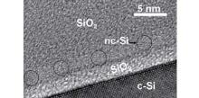
It is believed that the excessive Si would precipitate into clusters which are crystallized during thermal annealing. According to the constrained crystallization model, [14] the size of the Si-NCs could be controlled accurately. The Raman measurements show that a narrow peak at 515.2 cm− 1 appears in the spectra of the annealed samples, which demonstrates the formation of Si-NCs during thermal annealing. The detailed Raman results are not shown here but can be found in our previous studies.[15] The cross-sectional HRTEM image of annealed SiO2/Si-NCs in SiNx/SiO2/c-Si structure is shown in Fig. 1. Clear crystalline lattices of Si-NCs can be observed and the diameter (3 nm) of the dots is close to the thickness of as-deposited Si-rich silicon nitride layer. The HRTEM image confirms that the sandwiched structure (SiO2/Si-NCs in SiNx/SiO2) has been well fabricated. C– V, G– V, and I– V measurements have been performed by using an Agilent B1500 semiconductor parameter analyzer with a C– V measurement module.
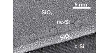 | Fig. 1. Cross sectional HRTEM image of annealed SiO2/Si-NCs in SiNx/SiO2/c-Si structure. |
3. Results and discussion
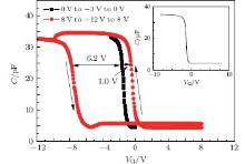
Figure 2 shows the C– V characteristics of our samples containing Si-NCs. The scanning voltage rate is 0.25 V/s. Both the delay time and measurement time are set to 0.1 s for each voltage step of 50 mV. The double sweep starts from 8 to – 12 V (backward scan) and returns to 8 V (forward scan). An obvious counterclockwise hysteresis is observed, indicating that both the electrons and holes can be injected from Si substrate into Si-NCs respectively. However, we can not see any hysteresis phenomenon in the reference sample under the same measurement conditions (inset in Fig. 2). Therefore, the hysteresis should be attributed to the charge storage in the Si-NCs and/or traps related to Si-NCs. Compared to the initial flat band voltage (VFB) of uncharged state, it is found that the Δ VFB due to full charged holes (∼ 6.2 V) is much larger than that due to full charged electrons (∼ 1.0 V). To manifest this large difference, carefully designed C– V and I– V sweeps have been performed to investigate the detailed charging behaviors of electrons and holes separately.
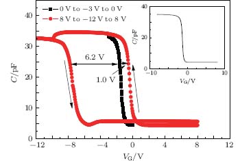 | Fig. 2. C– V hysteresis is obtained by sweeping from 8 to − 12 V and return. The initial VFB (∼ − 1.5 V) is also obtained by sweeping in a small range (0 to − 3 V). The inset is the C– V characteristics for the reference sample. |
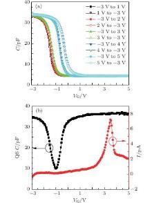
First, we focus on the electron charging and discharging processes using multiple double sweeps. To avoid the influence of holes, each double sweep starts from − 3 V to the end voltage (forward scan), and returns to − 3 V (backward scan). The end voltage is small initially and increases gradually to 5 V where the surface of substrate goes into a stronger inversion state. Figure 3(a) shows the C– V hysteresis due to electron charging process. As can been seen, Δ VFB is zero for the end voltage of 1 V. A small hysteresis appears for the end voltage of 2 V, indicating that the electrons injection has occurred. When the end voltage reaches 3 V, an abrupt Δ VFB appears. Next double sweep with the end voltage of 4 V shows the same C– V curve as that of 3 V during backward scan. The subsequent double sweep with the end voltage of 5 V exactly follows the one of 4 V. It means that the electron charging reaches saturation.
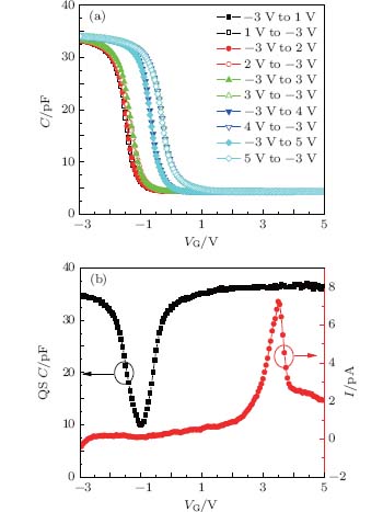 | Fig. 3. (a) Multiple double C– V sweeps from − 3 V to the end voltage and return. The end positive voltage increases from 1 to 5 V. Solid or open symbols used for forward scan or return. (b) Plots of gate current (circle) and quasi-static capacitance (square) verse the gate voltage. The sweep is performed from − 3 to 5 V. |
For the electron charging process, the I– V sweep (from − 3 to 5 V) with the same scanning voltage rate is performed, as shown in the right side of Fig. 3(b). An obvious upward peak appears. We suggest that the current peak is due to electron charging displacement current.[16, 17] The quasi-static capacitance of the sample was also derived from the estimation of displacement current made by the Agilent B1500, which is shown in the left side of Fig. 3(b). As can be seen, the threshold voltage (VTH), above which the electron charging peak can be observed, is about 2 V, indicating that electrons start injection at an electric field about 1.2 MV/cm in the deep inversion region. Therefore, we can not find any hysteresis in the C– V double sweep with the end voltage of 1 V.
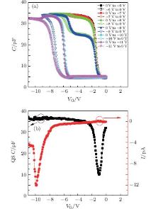
Next, we investigate the hole charging and discharging processes. Similar multiple double C– V sweeps are also performed, as shown in Fig. 4(a). Each double sweep starts from 0 V to the end voltage (backward scan), and returns to 0 V (forward scan). The end negative voltage is small initially and increases gradually to − 11 V. The hysteresis can not be observed until the end voltage reaches − 7 V, where a small distortion appears. When the end voltage is − 8 V, a distorted C– V curve with an obvious capacitance plateau can be found during forward scan. When the end voltage is − 10 V, the C– V curve distortion disappears and the VFB shifts to more negative voltage. The C– V sweep with the end voltage of − 11 V is the same as the one of − 10 V, indicating that the hole charging reaches saturation.
 | Fig. 4. (a) Multiple double C– V sweeps from 0 V to the end voltage and return. The end negative voltage increases from − 6 V to − 11 V. Solid or open symbols used for backward scan or return. (b) Plots of gate current (circle) and quasi-static capacitance (square) verse the gate voltage. The sweep is performed from 0 V to − 11 V. |
For the hole charging process, the quasi-static C– V and I– V sweeps (from 0 to − 11 V) are shown in Fig. 4(b). An obvious downward peak appears which should be attributed to the hole charging displacement current. The VTH, above which the hole charging peak can be observed, is about − 7 V, indicating that holes start injection at electric field about 1.8 MV/cm in the deep accumulation region.
Comparing Figs. 3 and 4, we can see that the charging characteristics between electrons and holes are different: not only the full charged Δ VFB but also the shape of the C– V curve (reflecting the charging process). We will use the G– V measurements, which were carried out simultaneously with the C– V measurements, to study the nature of the difference.
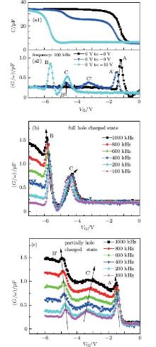
It is well known that the G– V characteristics are accurately sensitive to interface defect states. Figures 5(a1) and 5(a2) show C– V and G– V curves during forward scan for the electron charging process. We find that the position of G– V peaks correspond to the C– V transition region and is close to the VFB. The shift of the G– V peak between uncharged state and charged state of electron is almost equal to the shift of VFB. Figures 5(b) and 5(c) show the frequency dependence of G– V characteristics at the uncharged state and the charged state of electron (VFB ∼ 0.8 V), respectively. It is found that the FWHM of both peaks does not change with increasing the measurement frequency, but the peak position shifts to negative direction. This negative frequency dependence of the G– V peak position is the typical characteristics of the admittance peak originated from the interface states between the SiO2 and the Si substrate.[18– 20] It should be noted that after electrons start injection, the interface states at SiO2/Si-substrate do not influence the electron charging process.
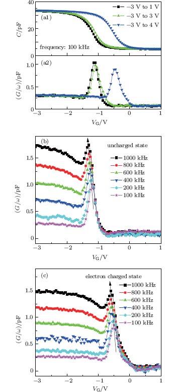 | Fig. 5. C– V (a1) and G– V (a2) characteristics during forward scan for the electron charging process. (b) Frequency dependence of G– V characteristics at the uncharged state. (c) Frequency dependence of G– V characteristics at the charged state of electron. |
However the G– V characteristics of hole charging process are much different from that of the electron charging process. Figures 6(a1) and 6(a2) show C– V and G– V curves during backward scan for the hole charging process. We can see that for the uncharged state (sweeping from 0 to − 6 V) there is also a G– V peak (marked as A) which is the same as that of the uncharged state in Fig. 5(a2). But for the full charged state of hole (sweeping from 0 to − 10 V), there are two G– V peaks (marked as B and C) which are obviously different from that of the charged state of electron in Fig. 5(a2). Moreover, for the partially charged state of hole (sweeping from 0 to − 9 V), where the abnormal C– V plateau appears as shown in Fig. 4(a), there are three G– V peaks (marked as A', B', and C'). In order to further investigate why more G– V peaks can be generated during the hole charging process and what is the origination of these G – V peaks, we also use the characteristics of frequency dependent G– V peak position to identify these G– V peaks. Figure 6(b) shows the frequency dependence of G– V peaks B and C at the full charged state. It is clearly shown that the peak B exhibits negative frequency dependent characteristics, which is response of interface states at SiO2/Si-substrate. However, peak C exhibits positive frequency dependent characteristics, which is due to the response of the oxide hole traps in the oxide layer.[20] The influence of oxide hole traps can be further supported by Fig. 6(c). In the Fig. 6(c), we can see that both of peaks A' and B' have negative frequency dependent characteristics, but peak C' has positive frequency dependent characteristics, which is the same as that of peak C at the full charged state in Fig. 6(b). On the other hand, the FWHM of peak C' is getting wider when the frequency increases, which means that trapped holes can not response to higher frequency. When the sweeping voltage gets higher than − 9 V, the trapped holes can not be sustained to the oxide traps and the excess holes are transferred to the Si-NCs, while the G– V peak C' simultaneously evolves to peak C and peak B' evolves to peak B. Consequently, the capacitance plateau disappears and C– V curves restore to their normal shape.
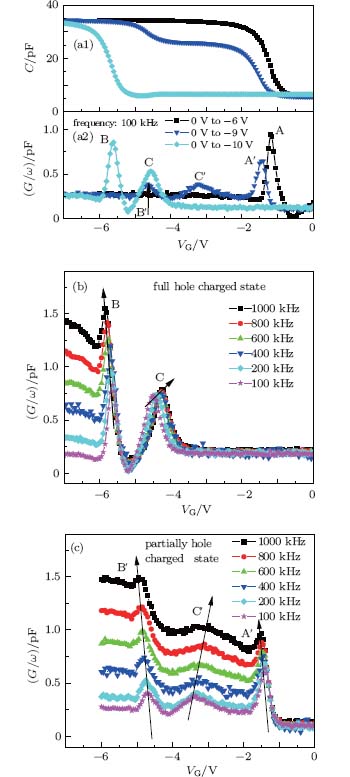 | Fig. 6. C– V (a1) and G– V (a2) characteristics during backward scan for the hole charging process. (b) Frequency dependence of G– V characteristics at the full charged state of hole. (c) Frequency dependence of G– V characteristics at the partially charged state of hole. |
The present results indicate that the electrons charging occurs within the Si-NCs away from the oxide trap defects, while holes are initially trapped to oxide traps near the interface of the SiO2/Si-substrate and the excess holes are transferred to the Si-NCs. This results in the abnormal C– V characteristics. Therefore, the Δ VFB due to full charged holes is contributed by both of Si-NCs and oxide hole traps.
4. Conclusion
The electrons and holes charging characteristics in the floating gate structure of SiO2/Si-NCs in SiNx/SiO2/c-Si have been systematically investigated. It is found that the hole charging process is different from that of electrons not only in the full charged Δ VFB but also in the shape of the C– V curves. The results of C– V and G– V measurements indicate that the hole charging occurs via a two-step tunneling mechanism which is caused by the near-interface oxide traps. This different charging behavior may help us to evaluate the quality of tunneling oxide in the Si-NCs floating gate NVM.
Reference
| 1 |
|
| 2 |
|
| 3 |
|
| 4 |
|
| 5 |
|
| 6 |
|
| 7 |
|
| 8 |
|
| 9 |
|
| 10 |
|
| 11 |
|
| 12 |
|
| 13 |
|
| 14 |
|
| 15 |
|
| 16 |
|
| 17 |
|
| 18 |
|
| 19 |
|
| 20 |
|