Degradation mechanism of enhancement-mode AlGaN/GaN HEMTs using fluorine ion implantation under the on-state gate overdrive stress*
Cite this Article
Sun Wei-Wei, Zheng Xue-Feng, Fan Shuang, Wang Chong, Du Ming, Zhang Kai, Chen Wei-Wei, Cao Yan-Rong, Mao Wei, Ma Xiao-Hua, Zhang Jin-Cheng, Hao Yue. Degradation mechanism of enhancement-mode AlGaN/GaN HEMTs using fluorine ion implantation under the on-state gate overdrive stress* . Chinese Physics B, 2014, 24(1): 017303 
Permissions
Degradation mechanism of enhancement-mode AlGaN/GaN HEMTs using fluorine ion implantation under the on-state gate overdrive stress*
Corresponding author. E-mail: xfzheng@mail.xidian.edu.cn
Project supported by the National Natural Science Foundation of China (Grant Nos. 61334002, 61106106, and 61474091), the Opening Project of Science and Techology on Reliability Physics and Application Technology of Electronic Component Laboratory (Grant No. ZHD201206), the New Experiment Development Funds for Xidian University, China (Grant No. SY1213), and the Scientific Research Foundation for the Returned Overseas Chinese Scholars.
Abstract
The degradation mechanism of enhancement-mode AlGaN/GaN high electron mobility transistors (HEMTs) fabricated by fluorine plasma ion implantation technology is one major concern of HEMT’s reliability. It is observed that the threshold voltage shows a significant negative shift during the typical long-term on-state gate overdrive stress. The degradation does not originate from the presence of as-grown traps in the AlGaN barrier layer or the generated traps during fluorine ion implantation process. By comparing the relationships between the shift of threshold voltage and the cumulative injected electrons under different stress conditions, a good agreement is observed. It provides direct experimental evidence to support the impact ionization physical model, in which the degradation of E-mode HEMTs under gate overdrive stress can be explained by the ionization of fluorine ions in the AlGaN barrier layer by electrons injected from 2DEG channel. Furthermore, our results show that there are few new traps generated in the AlGaN barrier layer during the gate overdrive stress, and the ionized fluorine ions cannot recapture the electrons.
Keyword:
73.61.Ey; 85.40.Ry; 78.30.Fs; E-mode HEMTs; gate overdrive; electron injection; impact ionization
1. Introduction
Due to the high-electric breakdown field and high-density polarization-induced two-dimensional electron gas (2DEG) channel, [1– 3] wide bandgap AlGaN/GaN high electron mobility transistors (HEMTs) are promising candidates for next-generation microwave power amplifiers and high-voltage switches, especially in high temperature, high power, and irradiation resistant environments.[4– 8] Generally, conventional AlGaN/GaN HEMTs are depletion mode (D-mode) transistors with negative threshold voltage. Concerning the practical applications, however, there is a pressing need for enhancement mode (E-mode) HEMTs with positive threshold voltage, especially for two important applications: power switching converters and digital logic circuits.[9– 11] Up to now, great efforts have been made to explore the fabrication technology of E-mode HEMTs, [12, 13] such as by thinning the AlGaN barrier layer, [14] the structure of groove gate, [15] p-type gate electrode, [16] etc. Among these technologies, the fluoride-based plasma treatment is a very important approach to realize E-mode HEMTs.[17] By utilizing it, the negatively charged fluorine (F) ions can be implanted into the AlGaN barrier, which can effectively deplete the 2DEG in the channel under the gate.[18] Then the threshold voltage changes from negative value to positive value, and E-mode HEMTs are realized.
Reliability is a major issue for both D-mode and E-mode HEMTs. Especially for E-mode HEMTs, the stability of F ions in the barrier layer may cause serious reliability problems under certain application environments. Yi et al. have investigated the degradation of F plasma treatment devices under OFF-state and ON-state long-term stress. A negative shift of the threshold voltage was observed after 288 hours of stress.[19] In the applications of power switch and microwave amplifier, the Schottky gate electrode of E-mode HEMTs may be forward biased with a high positive voltage, which will cause significant hot electron injection from the 2DEG channel. To study the degradation mechanism of E-mode HEMTs under so-called on-state gate overdrive stress, which features a high positive gate bias with a low positive drain bias, some related research work has been carried out. Chen et al. claimed that the degradation mechanism can be explained by the impact ionization of F ions in the barrier layers under the gate.[20] However, more experimental evidences are highly required to validate this proposed physical model.
In this paper, typical on-state gate overdrive stress experiments are performed to investigate the degradation mechanism of E-mode HEMTs. The effects of as-grown traps and generated traps during fluoride-based plasma treatment in the AlGaN barrier layer on degradation have been studied. The correlations between the shift of threshold voltage and the amount of injected electrons under different stress conditions have been compared, which provides valuable information for the understanding of the degradation mechanism of E-mode HEMTs. Moreover, the effects of gate overdrive stress on the generation of new traps and on the properties of the ionized fluorine ions are also discussed.
2. Devices and experiments
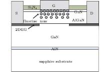
The AlGaN/GaN HEMT structure used in this paper was grown on a (0001) sapphire substrate by metal-organic chemical vapour deposition (MOCVD). The HEMT structure consists of an AlN nuclear layer, a 1.3-μ m-thick unintentionally doped GaN buffer layer, and a 20-nm-thick undoped Al0.3Ga0.7N barrier layer, with a 1-nm-thick in-situ growth GaN cap layer. Room-temperature Hall measurements show an electron sheet density of 1.1 × 1013 cm− 2. The device fabrication starts with the source/drain ohmic contact formation. Ohmic contacts consisting of Ti/Al/Ni/Au (20 nm/180 nm/55 nm/45 nm) were annealed in ambient nitrogen at 850 ° C for 30 s, with a contact resistance about 0.5 Ω · mm. Then the device mesa isolation was performed using Cl2/Ar plasma dry etching in a reactive ion etching (RIE) system. In the following, surface passivation was carried out by depositing about 60-nm Si3N4 through the plasma-enhanced chemical vapor deposition (PECVD). The recessed-gate area was formed by contact lithography, [21] which was followed by CF4 plasma treatment in an RIE system at a radio frequency plasma bias voltage of 150 V. The effective density of the implanted F ion is around 9.6 × 1012 cm− 2. After a post-gate rapid thermal annealing (RTA) at 350 ° C for 5 minutes, Ni/Au deposition and liftoff were performed to form the electrodes. The gate length and width of HEMTs are 0.6 μ m and 20 μ m, respectively. Both the gate– source spacing Lgs and gate-to-drain spacing Lgd are 1.4 μ m. Figure 1 shows the schematic cross section of E-mode HEMTs based on F ion implantation technology in this study. For further comparison, D-mode HEMTs were also fabricated on the same wafer without F ion implantation to the recessed-gate area.
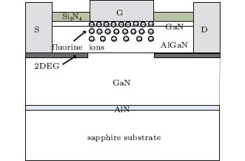 | Fig. 1. Schematic cross section of E-mode HEMTs fabricated by fluoride-based implantation technology. |
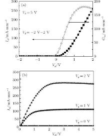
The incorporation of negatively charged F ions into the AlGaN barrier layer can effectively deplete the electrons in the 2DEG channel under the gate. The test equipment used in this experiment is Agilent B1500 semiconductor parameter tester. Figure 2 presents the initial transfer characteristic (TC) and output characteristic of the E-mode HEMT used in this work. It is observed that the fresh device feathers a threshold voltage (Vth) of 0.55 V and a peak transconductance (Gmmax) of 180 mS· mm-1.
 | Fig. 2. (a) Transfer characteristic and (b) output characteristic of a fresh E-mode HEMT in this paper. Vth = 0.55 V and Gmmax = 180 mS· mm− 1. |
During experiments in this paper, TC measurement is first carried out to evaluate the initial properties of the test HEMTs. Then the device is biased under the on-state gate overdrive stress for a pre-set time. The stress is interrupted at the pre-set intervals, then the threshold voltage and the level of electron injection are monitored against time. The stress is terminated when the pre-set stress time is reached.
3. Results and discussion
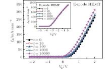
A typical on-state gate overdrive stress of Vg = 3.0 V with Vds = 1.0 V (Ig = 350 mA· mm− 1) is selected and applied on an E-mode HEMT. As shown in Fig. 3, the TC curve is shifted along the Vg axis, suggesting the negative shift of Vth with increasing stress time. However, the transconductance changes little during the stress. In order to understand the degradation mechanism of this phenomenon, three possible reasons are examined in the following.
 | Fig. 3. Transfer characteristic curves on a fresh E-mode HEMT under a typical on-state gate overdrive stress (Vg = 3.0 V, Vd = 1.0 V, Ig = 350 mA· mm− 1). The maximum stress time is up to 10 ks. In comparison, the TC curves on a D-mode HEMT fabricated on the same wafer under the identical gate injection current (Ig = 350 mA· mm− 1) are also shown in the inset. |
(i) As-grown traps in AlGaN barrier layer To explore the possibility of whether the negative shift of Vth is caused by the detrapping of as-grown traps in the barrier layer, the identical electric stress is applied on a D-mode HEMT with the same size and structure except the F ions implantation process. If the observed degradation is caused by the detrapping of as-grown electron traps, the same negative shift of Vth should be observed on the D-mode HEMT. However, as illustrated in the insert of Fig. 3, no evident shift is observed for the TC curves of the D-mode HEMT, which indicates that there are little as-grown traps in AlGaN barrier layer.
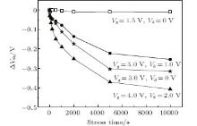
(ii) Generated traps during F ion implantation process To realize E-mode HEMTs, F ions with enough energy are implanted into the AlGaN layer in this work. These F ions work as negative charges to deplete the 2DEG channel under the gate. On the other hand, they damage the lattice of AlGaN layer and may generate new traps. In general, most of these new traps can be reduced effectively by annealing at a proper temperature. To verify whether there are some residual traps that cannot be annealed in the AlGaN layer, a trap filling procedure is applied to the fresh E-mode HEMT, which consists of a considerate forward gate bias (Vg = 1.5 V) with source and drain terminals be grounded. It can provide a large electron injection to fill the new generated traps with few additional traps introduced. As shown in Fig. 4, no significant shift of the threshold voltage (Δ Vth) is observed even when the filling time is up to 10 ks. We can conclude that the traps generated during the F ion implantation process are negligible.
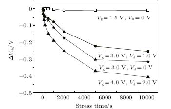 | Fig. 4. Shifts of threshold voltage (Δ Vth) on E-mode HEMTs under different on-state stress conditions. The maximum stress time is up to 10 ks. |
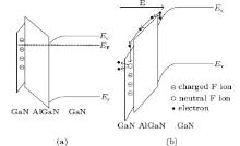
(iii) Impact ionization of F ions in AlGaN barrier layer Lastly, we will examine the third possible reason for the degradation mechanism of E-mode HEMTs under the gate overdrive stress. In early work, an impact ionization model of F ions in AlGaN barrier was proposed to explain this phenomenon. Figure 5(a) shows the energy band diagram of the AlGaN/GaN heterojunction in equilibrium state. When a forward gate bias is applied to the gate, according to this model, the free electrons in 2DEG channel can have enough energy to surmount the energy barrier at AlGaN/GaN interface and inject into the barrier layer. Then these injected electrons are accelerated, gain kinetic energy, and become high energy carriers, which have a possibility to ionize the negatively charged F ions. After ionization, some of the F ions lose negative charges and become neutral, which will weaken the depletion effect on 2DEG channel, as shown in Fig. 5(b). Then the threshold voltage of E-mode HEMT will have a negative shift.
 | Fig. 5. Schematic energy band diagram of the AlGaN/GaN heterojunction under (a) equilibrium state and (b) forward gate bias state, respectively. |
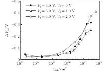
In terms of the theory of impact ionization, the ionization rate of charged ions has strong dependence on the amount of injected high energy carriers. To evaluate the validation of this impact ionization model, stresses with different on-state gate overdrive bias are carried out on E-mode HEMTs. Figure 4 shows the degradation of Vth during several typical biases. It is found that Vth decreases significantly at the beginning of stress, and then slows down with increasing stress time. Meanwhile, the injection current density during stress is also monitored and the corresponding cumulative injected electrons (Qinj) can be calculated. The curves of Δ Vth versus Qinj under different gate overdrive biases are plotted in Fig. 6. It is found that Δ Vth has strong dependence on the injected electron density, but is independent of the stress conditions that are used in this work. This result is observed for the first time and agrees with our expectation in the proposed impact ionization model, which provides important and direct experimental evidence to support it. We can therefore conclude that the negative shift of Vth in gate overdrive stress E-mode HEMTs is caused by the ionization of negatively charged F ions in the barrier layer. Further experiments show that the minimum impact ionization energy for F ions is around 1.8 eV in this work, which agrees with the results in previous work.[20]
 | Fig. 6. Δ Vth against Qinj under different on-state gate overdrive stresses on E-mode HEMTs. Qinj denotes the cumulative electrons injected during stress. |
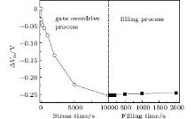
According to the theory of hot carrier injection, the high energy electrons injected from the 2DEG channel may also damage the AlGaN barrier and generate electron traps. To evaluate this possibility, a filling procedure with Vg = 1.5 V and Vds = 0 V is carried out immediately after the gate overdrive stress, which can provide enough free electrons to fill neutral electron traps without generating any additional traps. As shown in Fig. 7, the threshold voltage changes little even when the filling time is up to 2000 s, which indicates that the electron traps generated during gate overdrive stress are negligible. This agrees with the conclusion in the early work.[20] It has been reported that the gate leakage is not deteriorated even when Vth reveals an evident shift under typical gate overdrive stress in E-mode HEMTs, which indicates that few additional defects of traps are generated. Meanwhile, figure 7 also demonstrates that the ionized F ions cannot recapture electrons after losing negative charges with impact ionization, which agrees with the observed results in Si MOSFETs with electric field assisted annealing. It can be explained by the formation of Ga– F bonds, which is very stable even when the temperature is up to 400 ° C.[18]
 | Fig. 7. Effect of electron trap filling bias (Vg = 1.5 V, Vds = 0 V) on a gate overdrive stressed (Vg = 3.0 V, Vds = 1.0 V) E-mode HEMT. |
4. Conclusions
In this work, the degradation mechanism of AlGaN/GaN E-mode HEMTs fabricated by fluorine plasma ion implantation technology under the typical on-state gate overdrive stress has been systematically investigated. Combining with the trap characterization, the as-grown traps in AlGaN barrier layer and the traps generated during F ion implantation in E-mode HEMTs have been studied in detail and ruled out as the reasons. It has been found that the shift of threshold voltage depends strongly on the cumulative injected electrons, but is independent of the stress conditions applied to the E-mode HEMTs in this work. It provides direction experimental evidence to support the impact ionization model, in which the degradation mechanism of E-mode HEMTs under the gate overdrive stress can be explained by the ionization of F ions by the high kinetic energy electrons injected from the 2DEG channel. Furthermore, it is also found that the traps generated during the gate overdrive stress are negligible and the ionized F ions cannot recapture electrons.
Reference
| 1 |
|
| 2 |
|
| 3 |
|
| 4 |
|
| 5 |
|
| 6 |
|
| 7 |
|
| 8 |
|
| 9 |
|
| 10 |
|
| 11 |
|
| 12 |
|
| 13 |
|
| 14 |
|
| 15 |
|
| 16 |
|
| 17 |
|
| 18 |
|
| 19 |
|
| 20 |
|
| 21 |
|