

Influence of compressive strain on the incorporation of indium in InGaN and InAlN ternary alloys*
Cite this Article
Zhao Yi, Zhang Jin-Cheng, Xue Jun-Shuai, Zhou Xiao-Wei, Xu Sheng-Rui, Hao Yue. Influence of compressive strain on the incorporation of indium in InGaN and InAlN ternary alloys* . Chinese Physics B, 2014, 24(1): 017302 
Permissions
Influence of compressive strain on the incorporation of indium in InGaN and InAlN ternary alloys*
Corresponding author. E-mail: jchzhang@xidian.edu.cn
Project supported by the National Natural Science Foundation of China (Grant Nos. 61404099 and 61306017) and the Fundamental Research Funds for the Central Universities, China (Grant No. JB141101).
Abstract
In order to investigate the influence of compressive strain on indium incorporation in InAlN and InGaN ternary nitrides, InAlN/GaN heterostructures and InGaN films were grown by metal–organic chemical vapor deposition. For the heterostructures, different compressive strains are produced by GaN buffer layers grown on unpatterned and patterned sapphire substrates thanks to the distinct growth mode; while for the InGaN films, compressive strains are changed by employing AlGaN templates with different aluminum compositions. By various characterization methods, we find that the compressive strain will hamper the indium incorporation in both InAlN and InGaN. Furthermore, compressive strain is conducive to suppress the non-uniform distribution of indium in InGaN ternary alloys.
Keyword:
73.61.Ey; 73.40.Kp; 79.60.Jv; 78.70.Ck; compressive strain; indium incorporation; InAlN; InGaN
1. Introduction
InN-based III– V nitrides currently attract intensive attention for their potential device applications. For example, InGaN alloys have been widely adopted in light emitting diodes or laser diodes, [1] and are very promising for full-solar-spectrum high efficiency photovoltaic devices.[2] Since InAlN with 17% indium content can be grown lattice matched to GaN, thus an InAlN barrier has the potential to improve the reliability and performance of high electron mobility transistors (HEMTs).[3] Furthermore, improved electron mobility has been received in an InGaN-channeled HEMT with an InAlGaN quaternary barrier.[4] Nonetheless, owing to the significant distinctions in chemical and thermodynamics properties among AlN, GaN, and InN, the growth of a high-quality InN-based III– V alloy with arbitrary assigned indium content is challenging and very sensitive to epitaxial parameters. In addition, due to the absence of a lattice-matched substrate and the demand for heterojunction structures, III– V nitrides are often grown under strain, consequently, the growth of InN-based nitride is also affected by strain greatly. Previous research has shown that phase separation or composition fluctuation can be suppressed by residual strain in InAlN and InGaN alloys.[5, 6] Moreover, compositional pulling effects in thick InGaN films have been attributed to strain relaxation.[7] In most of the literature, the impact of compressive strain on InN-based nitride is investigated by charactering a film at different depths or studying quantum well structures grown on inserted InGaN underlying layers with varying thicknesses.[7, 8] In this study, the influence of compressive strain on the indium incorporation in InAlN and InGaN is concentrated on. For InAlN, different compressive strains are realized by respective growths of GaN templates on an unpatterned planar sapphire substrate (UPS) and patterned sapphire substrate (PSS) before InAlN growths; and for InGaN, AlGaN templates with different aluminum compositions as well as one GaN template were employed for the following InGaN growths. We find that InN mole fraction is reduced by enhanced compressive strain for both InAlN and InGaN alloys. Furthermore, compressive strain is indeed conducive to suppress the non-uniform indium distribution in InGaN alloys.
2. Experiment
Epitaxial growths were performed in our homemade metal– organic chemical vapor deposition (MOCVD) system. All the sapphire substrates including PSS were c-plane oriented, and the PSS is cone-shape patterned with the pattern diameter, height, and interval of 2 μ m, 1.5 μ m, and 1 μ m. Triethylgallium (TEG), trimethyaluminum (TMA), trimethylindium (TMIn), and ammonia were used as Ga, Al, In, and N precursors, respectively. Purified hydrogen was used as the carrier gas except for in the growth stage of InAlN or InGaN, during which the carrier gas was switched to nitrogen. For all the samples, AlN nucleation layers were deposited under identical conditions as mentioned in a previous report.[9] For InAlN samples, InAlN/GaN heterostructures were grown on UPS and PSS in the same run. The growth temperatures of InAlN and GaN were 720 ° C and 940 ° C, respectively, and the thickness of either InAlN layer was 13 nm, which was grown under the PMOCVD mode, [9] and actually played the role of a barrier. For InGaN samples, before the growth of InGaN films, AlGaN templates with different aluminum compositions were grown at above 1070 ° C, respectively. The varying aluminum compositions were realized by adjusting the reactant flux ratios of TMA to TEG. Another conventional GaN template was also prepared for comparison. Evidently, the compressive strain was enhanced by the increased aluminum content in the template. Finally, 100-nm InGaN layers were deposited on various templates simultaneously. Van Der Pauw Hall measurement was employed to determine the two-dimensional electron gas (2DEG) density formed at the InAlN/GaN heterojunction interface. The compressive strains in GaN buffer layers on UPS and PSS were analyzed by Raman scattering spectroscopy (Raman). Indium contents in InAlN or InGaN samples were evaluated by x-ray diffraction (XRD). In addition, for InGaN samples, photoluminescence (PL) was also utilized to investigate the variation tendency of InN mole fractions with compressive strains using the 325-nm line of a He– Cd laser.
3. Results and discussion
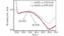
At first, 2DEG densities were measured to be 2.1208× 1013 cm− 2 and 1.9822× 1013cm− 2 by Hall for the InAlN/GaN samples grown on UPS and PSS, respectively. Obviously, there is a 2DEG density difference of 1.386× 1012 cm− 2 between the two samples. It is well known that for the III-nitride heterostructure, 2DEG is closely associated with the total polarization strength (sum of the spontaneous polarization and the piezoelectric polarization) in the barrier. Consequently, variation of 2DEG density should be accompanied by an altered total polarization strength. For the InAlN barrier, the total polarization strength will be enhanced by the increased aluminum content and hence 2DEG with a higher density is achieved. Therefore, we deduce that the InAlN/GaN heterojunction grown on UPS should possess higher (or lower) AlN (or InN) mole fraction than the one on PSS. In order to confirm our deduction, indium contents in both barrier layers were estimated by XRD and the ω – 2θ scan patterns around the (0002) reflection are plotted in Fig. 1. The diffraction peaks at 35.1347° and 35.1736° correspond to the InAlN films grown on PSS-GaN and UPS-GaN, respectively, confirming the existence of composition difference between the two InAlN barriers. Utilizing the computing method and parameters presented in Ref. [10], the difference of 2DEG densities between the two heterostructures due to the different total polarization strengths in the two InAlN barrier layers is calculated to be 1.373× 1012 cm− 2, which is quite close to the 1.386× 1012cm− 2 obtained by Hall measurement. The slight deviation between calculation and Hall measurement may originate from rounding or measuring errors and the controversial elastic constants of wurtzite III-nitrides adopted during calculations as well. Overall, combining the analysis and calculation, it is reasonable to expect that the difference of 2DEG densities originates from the altered aluminum (or indium) compositions in the InAlN barriers.
 | Fig. 1. XRD ω – 2θ scan patterns around the (0002) reflection from both InAlN/GaN heterostructure samples grown on UPS and PSS. |
Since both InAlN barriers were grown simultaneously, the discrepancy between chemical components cannot be ascribed to the undulation of growth batches. Pereira et al.[7] have shown that strain could have an effect on the composition during the growth of the nitride alloy. Hence the different chemical components in InAlN barriers ought to be concerned with the influence of unequal strains introduced by GaN buffer layers on PSS and UPS.[11] In order to investigate the residual strain in the GaN buffer layer, Raman measurement was adopted and the result is shown in Fig. 2. In Fig. 2, the E2(high) photon frequencies of GaN buffer layers grown on PSS and UPS are 572.3 and 573.7cm− 1, respectively, indicating that the GaN layer on PSS has undergone less compressive strain than the one on UPS. The relatively alleviative compressive strain is owing to the ELOG-like growth mode of GaN on PSS.[11] Therefore, through our study, for InAlN alloy, the compressive strain will hinder the incorporation of indium and thus lower the indium content. Although Lorenz et al.[12] have reported that compressive strain seems to facilitate the InN incorporation in InAlN; however, their samples are much thicker than ours, consequently effecting the quality degeneration of thick InAlN film, but strain relaxation may also be the origin of InN mole fraction variation.
 | Fig. 2. Raman spectra of both InAlN/GaN heterostructure samples grown on UPS and PSS with a partial enlarged image shown in the inset. |
PL is a powerful method to characterize the constituent and property of III– V nitrides. However, for the above-mentioned high-aluminum InAlN films, the InN mole fractions cannot be determined by the PL system equipped with a 325-nm laser, whose energy is too low to realize excitation. In order to further investigate the impact of compressive strain on the indium incorporation into InN-based ternary nitrides by PL, InGaN-film samples were grown on AlGaN templates with increasing aluminum compositions (named as sample B, C, and D, and the corresponding designed AlN mole fraction is 10% , 15% and 20% , respectively), another sample on GaN template was also adopted for comparison (named as sample A). All the InGaN films were also grown simultaneously to avoid fluctuation from different batches. Figure 3 shows the PL spectra of the InGaN samples. For sample A, besides the peaks related to InGaN, the peaks at around 364 and 728 nm are assigned to GaN template and its harmonic, respectively. There is strong composition fluctuation in sample A according to PL, furthermore, indium– metal droplets can be observed at the sample surface by an optical microscope. For any other InGaN samples, no signal from AlGaN template is detected due to the relatively large band-gap. For sample D, there is distinct energy splitting, which is evidence of strain relaxation, the secondary lower-energy PL component is introduced by the discontinuous strain relaxation when the critical layer thickness (CLT) is exceeded.[13] With increasing aluminum contents in the templates from sample B to D, InGaN layers are grown under increasing compressive strain, and the PL emission peaks shift to higher energy. This blue-shift is caused by the reduced InN mole fraction as the strain increases, implying that the compressive strain will hinder the indium incorporation into InGaN. However, there may be some puzzle that compared with sample A grown on a GaN template, the PL curve of sample B on an AlGaN template shows a somewhat red-shift. We attribute this phenomenon to composition fluctuation and indium segregation, both of which hamper the effective incorporation of indium and thus lower the InN mole fraction in sample A. On the contrary, thanks to the AlGaN template used in sample B, composition fluctuation and indium segregation is suppressed by the enhanced compressive strain, [6] which assists the increase of indium content to some certain extent. Nevertheless, it should be emphasized that the InN mole fraction will begin to decline if the compressive strain is enhanced further, as shown in Fig. 3.
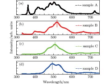 | Fig. 3. PL spectrums of different InGaN samples: (a) sample A, (b) sample B, (c) sample C, and (d) sample D. |
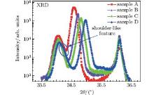
The influence of compressive strain on the incorporation of indium into InGaN was also investigated by XRD. In Fig. 4, XRD ω – 2θ scan patterns around (0002) reflection of all InGaN samples are presented. Besides the peaks of AlN nucleation layers, the peaks originated from AlGaN or GaN templates can be clearly distinguished and shift to higher angles with increasing aluminum composition. The InGaN-related peaks locate at 34.0533° , 34.0456° , 34.0728° , and 34.0971° for samples A, B, C, and D, corresponding to InN mole fractions of 14.42% , 14.64% , 13.85% , and 13.15% , respectively. The variation of XRD data is in good accordance with the results of PL. From the XRD measurements, the InN mole fraction of sample A is less than that of B as well, which has been interpreted as the results of composition fluctuation and indium segregation in sample A; meanwhile, the InN mole fractions decrease with increasing compressive strain from sample B to C to D. It should be noted that there is a shoulder-like feature at the right side of the InGaN peak in sample D, which is also evidence of strain relaxation according to the publication of Pereira et al.[14] and corresponding to the double-peak structure observed in the PL pattern of sample D. Therefore, based on both PL and XRD characterizations, we conclude that compressive strain has an important effect on the growth of InGaN ternary alloy, which could not only suppress the non-uniform distribution of InN mole fraction but also affect the indium incorporation into InGaN alloy.
 | Fig. 4. XRD ω – 2θ scan patterns around (0002) reflection of InGaN film samples A, B, C, and D. The AlN mole fraction in the AlGaN templates of samples B, C and D are determined to be 9.71% , 15.99% , and 21.46% , coincided with the designed compositions. |
4. Conclusions
In conclusion, combining the aforementioned research results of InAlN and InGaN samples, compressive strain does play an effect on the indium incorporation into InN-based ternary alloys. For the growth of either InAlN or InGaN alloy, InN mole fraction will decrease gradually with the increase of the compressive strain. In addition, the compressive strain could indeed suppress the non-uniform distribution of indium in InGaN ternary alloys, such as composition undulation, formation of an indium droplet, and phase segregation. Consequently, for the growth and characterization of InN-based ternary alloy, the influence of compressive strain on the material must be under consideration.
Reference
| 1 |
|
| 2 |
|
| 3 |
|
| 4 |
|
| 5 |
|
| 6 |
|
| 7 |
|
| 8 |
|
| 9 |
|
| 10 |
|
| 11 |
|
| 12 |
|
| 13 |
|
| 14 |
|