

Tunable terahertz plasmon in grating-gate coupled graphene with a resonant cavity*
Cite this Article
Yan Bo, Yang Xin-Xin, Fang Jing-Yue, Huang Yong-Dan, Qin Hua, Qin Shi-Qiao. Tunable terahertz plasmon in grating-gate coupled graphene with a resonant cavity* . Chinese Physics B, 2014, 24(1): 015203 
Permissions
Tunable terahertz plasmon in grating-gate coupled graphene with a resonant cavity*
Corresponding author. E-mail: hqin2007@sinano.ac.cn
Project supported by the National Natural Science Foundation of China (Grant No. 61271157), Jiangsu Planned Projects for Postdoctoral Research Funds, China (Grant No. 1301054B), and Suzhou Industry and Technology Bureau, China (Grant No. ZXG2012024).
Abstract
Plasmon modes in graphene can be tuned into resonance with an incident terahertz electromagnetic wave in the range of 1–4 THz by setting a proper gate voltage. By using the finite-difference-time-domain (FDTD) method, we simulate a graphene plasmon device comprising a single-layer graphene, a metallic grating, and a terahertz cavity. The simulations suggest that the terahertz electric field can be enhanced by several times due to the grating–cavity configuration. Due to this near-field enhancement, the maximal absorption of the incident terahertz wave reaches up to about 45%.
Keyword:
52.65.–y; 52.40.–w; 73.20.Mf; 87.50.U–; finite-difference-time-domain simulation; graphene; plasmon; terahertz
1. Introduction
Plasmons, a form of collective charge density oscillation, have attracted enormous interests in the development of new optoelectronic devices.[1– 3] Graphene is one kind of novel two-dimensional (2D) material in which the charge carriers are Dirac fermions.[4] Plasmons in graphene exhibit many unusual behaviors, including high wave velocity[5] and long propagation distance.[6] Both theoretical[5, 7, 8] and experimental[9– 11] studies have shown that the plasmon frequency of graphene falls in the terahertz and infrared region of the electromagnetic (EM) spectrum, and can be continuously tuned via the field effect when the charge density is varied in the range of 1011 cm− 2 to 1013 cm− 2. Furthermore, the plasmon absorption can be observed at room temperature in a graphene-based device rather than at cryogenic temperatures for the conventional two-dimensional electron gas (2DEG). Recently, great efforts have been made in the investigation of terahertz detectors [12] and modulators[13] based on the graphene 2DEG. However, the weak coupling between the plasmon modes and the incident terahertz wave hinders the development of practical terahertz plasmonic devices.[10, 12, 13] Hence, it is crucial to enhance the coupling. Many different micro-sized graphene structures, such as graphene ribbon arrays[9] and graphene disk arrays, [10] have been used to try to realize the strong excitation of plasmon modes in graphene. Here, we report simulation results of strong terahertz absorption by plasmon excitation in a grating coupled graphene embedded in a Fabry– Pé rot cavity. Metallic grating is used as a superior coupler and a top gate electrode, and the interaction between the graphene 2DEG and the EM wave can be enhanced by using the Fabry– Pé rot cavity. Similar schemes have been successfully applied in the conventional 2DEG.[14– 16] Finite-difference-time-domain (FDTD) simulations suggest that a remarkable absorption of terahertz EM wave is expected when the incident THz wave is in resonance with a specific graphene plasmon mode.
2. Model and approach
Three main building blocks are involved in this device, i.e., a Fabry– Pé rot cavity, a grating, and a graphene sheet, as shown in Fig. 1(a). The main body of the cavity is built on a Si substrate (ε 1 = 11.9) with a 300 nm SiO2 layer (ε 2 = 4) on top. The thickness of the Si substrate is hSi. A 20 nm-thick Al2O3 film (ε 3 = 6) is introduced between the graphene and the grating to serve as the top gate dielectric layer. The grating made of 200 nm thick gold with a conductance of 4.09 × 10⁷ S couples the cavity EM field with the graphene plasmon, the conductance is high enough to be viewed as a superconductor even in the THz region, thus the ohmic loss of the metal is small and ignorable. The width W and the period L of the grating gates as well as the gate voltage determine the plasmon modes which could be in resonance with the cavity THz EM modes. The distance between the graphene and the grating gates, d = 20 nm, affects the coupling strength, i.e., the smaller the distance, the stronger the coupling.
 | Fig. 1. (a) Schematic diagram of the proposed device that combines a grating coupled graphene with a Fabry– Pé rot cavity. (b) The frequency of the basic graphene plasmon mode as a function of the top-gate voltage. The inset shows the real part (ε ′ , black dash line) and the imaginary part (ε ″ , red solid line) of a bare graphene sheet with W = 3 μ m at VG = ± 2.67 V, corresponding to a charge density of 4.69 × 1012 cm− 2. |
The response of the graphene to the incident THz wave can be described by the dielectric function ε (ω ) = ε ∞ − iσ 2D/ε 0ω Δ , where σ 2D is the sheet conductivity of the graphene, ε ∞ = 1, ε 0 = 8.85 × 10− 12 F/m, and Δ = 0.5 nm represent the high frequency dielectric constant, the vacuum dielectric permittivity, and the thickness of the graphene layer, respectively. The excitation of the graphene plasmons by the incident THz wave can be described by the sheet conductivity as[10, 17]
 |
where ω is the angular frequency of the incident THz wave, ω p is the plasmon frequency, the carrier density n is related to the residual carrier concentration n0 and the top-gate voltage VTG by 

 |
where q is the plasmon wave vector, the Fermi energy is given by 

FDTD simulations are conducted to obtain the transmission and reflection characteristics of the proposed device at different gate voltages. The boundary conditions in directions x and z are set separately as periodic and perfectly-matched-layer (PML), respectively. A frequency-domain field profile is defined to map the distribution of the electric field. Transmission and reflection monitors are defined on both sides of the device so that the transmission and the reflection coefficients can be calculated.
3. Results and discussion
The plasmon frequency of a single-layer graphene coupled by the grating gates is calculated based on Eq. (2). For this calculation, we set m = 1, VDirac = 0 V, and n0 = 1 × 1012 cm− 2. As shown in Fig. 1(b), the graphene plasmon frequency characterizes bipolar and can be tuned between 1 THz and 4 THz by varying the top-gate voltage. By decreasing the length of the grating gates, the plasmon frequency can be increased accordingly.
A bare Fabry– Pé rot cavity with the grating gates but without the graphene layer is simulated to show the cavity EM modes. For the simulation, we choose W = 3 μ m, L = 6 μ m, and hSi = 200 μ m. The transmission spectrum is shown in Fig. 2(a). The periodic oscillations correspond to standing waves. The THz cavity modes are quantized as f = jc/2nsH with j = 1, 2, 3, … , [22] where c is the speed of light in a vacuum, and ns and H are the refractive index and the thickness of the cavity, respectively. The dependence of transverse electric field Ex at z = − 20 nm (the position of the graphene film) on the thickness of the resonant cavity is shown in Fig. 2(b), we confirm that the electric field near the edge under the grating can be several times larger than the incident radiation field. It is worth noticing that there is a maximum magnification at x = ± W/2. By changing hSi from 100 μ m to 400 μ m, the maximum magnification Ex/E0 varies from 8.87 to 1.39. Different grating structures on the top surface of the cavity induce various strong near-field enhancements, as shown in Figs. 2(c)– 2(e). The enhanced intensity enlarges with the gate width W and the duty ratio W/L increasing. Taking z = − 20 nm as an example, the enhancements with W/L = 0.5, W = 2 μ m; W/L = 0.5, W = 3 μ m; and W/L = 0.75, W = 3 μ m are 4, 5, and 8.4, respectively. Furthermore, besides the field component in the x direction, an enhanced field component in the z direction is induced near the edges of the gates. Due to the strong field enhancement, an effective coupling between the plasmon modes and the terahertz cavity modes can be achieved.
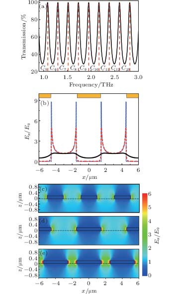 | Fig. 2. (a) Transmission spectrum of a device without graphene. The red dashed lines mark the resonant frequencies. (b) The transverse electric field Ex at f = 2.6 THz and z = − 20 nm. The blue dotted, red dashed, and black solid lines represent Ex/E0 for hSi = 100 μ m, 200 μ m, and 400 μ m, respectively. (c)– (e) Distributions of the transverse electric field Ex/E0 with different grating gates at f = 2.6 THz and hSi = 200 μ m. |
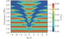
The simulated transmission spectra are shown in Fig. 3. Parameters W = 3 μ m, L = 6 μ m, hSi = 200 μ m, and Γ p = 1 THz are set in the simulation. The charge density n ranges from 1 × 1012 cm− 2 to 1.5× 1013 cm− 2, and the corresponding mobility μ is between 22000 cm2/(V· s) and 86000 cm2/(V· s). A few resonant transmission peaks (C7, C8, … , C11) split into lower branches (ω 7− , ω 8− , … , ω 11− ) and upper branches (ω 7+ , ω 8+ , … , ω 11+ ) when they intersect with the graphene plasmon dispersion curve (m = 1). The linewidths of the cavity mode (Γ C = 70 GHz) and the graphene plasmon modes (Γ p = 1 THz) can be directly extracted from the transmission spectra. The corresponding Q factors at fp = 1.53 THz (C7), 1.74 THz (C8), 1.95 THz (C9), 2.18 THz (C10), 2.39 THz (C11) are Qp = fp/Γ p = 1.53, 1.74, 1.95, 2.18, 2.39, respectively.
 | Fig. 3. Transmission spectra (W = 3 μ m, L = 6 μ m, hSi = 200 μ m) simulated at different gate voltages. The red and black dashed lines are plasmon modes (m = 1) and cavity modes (C5, C6, … , C11), respectively. |
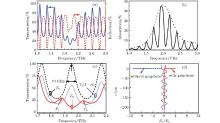
With the parameters set for Fig. 3, the transmission T and the reflection R spectra at fp = 1.95 THz are also obtained (Fig. 4(a)). The absolute absorption at the device mode can be given as A = 1 − T − R. The maximal absorption of this graphene device mode could be 45% (Fig. 4(b)). It is much larger than that of the bare graphene.[13] The transmission of the device mode with graphene (TG) near the resonant frequency is compared to that of the bare cavity (TC) and the change of the cavity transmission caused by the absorption (TC(1 − A)) in Fig. 4(c). It is expected that the transmission has an obvious decrease in the vicinity of the plasmon resonant frequency. Meanwhile, the transmission peak (C9) splits into a lower peak (Pl) and an upper peak (Pu) (see Fig. 4(c)). In order to explain the absorption of the incident light, we perform an FDTD simulation of the electric field distribution at the resonant frequency, as shown in Fig. 4(d). With the graphene in the middle, the amplitude of the transverse electric field becomes much smaller than that of the device mode without graphene. This characteristic is attributed to the absorption caused by the coupling between the cavity photon and the plasmon in graphene.
To design a practical terahertz device, two aspects of the graphene plasmon should be considered. First, the Q factor of the graphene plasmon, with Qp = fp/Γ p and 
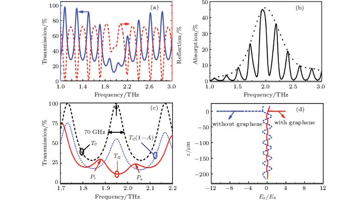 | Fig. 4. (a) Transmission and reflection spectra simulated by FDTD at fp= 1.95 THz, W= 3 μ m, L= 6 μ m, and hSi= 200 μ m. The blue solid and red dashed lines represent transmission and reflection, respectively. (b) The absolute absorption spectrum A= 1− T− R. (c) Transmission of the device mode without graphene TC, that with graphene TG, and transmission related to the absorption around 1.95 THz TC(1− A). (d) Simulation of the transverse terahertz electric field upon an incident transverse electric mode at x=W/2 corresponding to the 9th cavity mode (j=9). |
| Table 1. Parameters related to the terahertz plasmons for different gate widths at n = 1.5× 1013 cm− 2 and μ = 22000 cm2/(V· s). |
4. Conclusion
In this work, a graphene plasmon device that comprises a grating coupler and a THz cavity is investigated. Results show that the graphene plasmon frequency can be regulated between 1 THz and 4 THz by changing the gate voltage. Furthermore, the electric field is enhanced near the edges of the fingers, which strengthens the interaction between the graphene plasmon and the incident terahertz wave. Consequently, the maximal absorption of the incident wave in graphene can reach about 45%. By further improving the quality factor and the coupling with the graphene plasmon, graphene plasmon devices may find applications in THz modulators.
Reference
| 1 |
|
| 2 |
|
| 3 |
|
| 4 |
|
| 5 |
|
| 6 |
|
| 7 |
|
| 8 |
|
| 9 |
|
| 10 |
|
| 11 |
|
| 12 |
|
| 13 |
|
| 14 |
|
| 15 |
|
| 16 |
|
| 17 |
|
| 18 |
|
| 19 |
|
| 20 |
|
| 21 |
|
| 22 |
|