Charge trapping in surface accumulation layer of heavily doped junctionless nanowire transistors

Charge trapping in surface accumulation layer of heavily doped junctionless nanowire transistors |
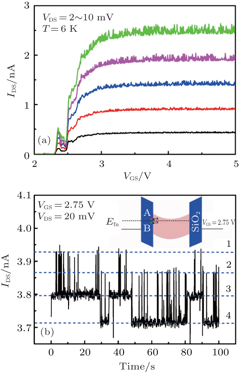
| Electrical performance of n-type JNT at low temperature of 6 K. (a) I DS– V GS curves for different V DS values from 2 mV to 10 mV in steps of 2 mV. (b) Time domain current levels. Typical segment of a full 100-s I DS versus time trace at V GS = 2.75 V and V DS = 20 mV. Four current levels observed at 6 K are ascribed to the capture and emission of electrons from two different traps. |
 |