


Optical properties of F- and H-terminated armchair silicon nanoribbons
[Lu Dao-Bang, Pu Chun-Ying, Song Yu-Ling† , Pan Qun-Na, Zhou Da-Wei, Xu Hai-Ru]
, Pan Qun-Na, Zhou Da-Wei, Xu Hai-Ru]
|
|


†Corresponding author. E-mail: yuling985@163.com
*Project supported by the Henan Provincial Joint Funds of the National Natural Science Foundation of China (Grant Nos. U1404608 and U1304612), the Science and Technology Key Projects of Henan Province, China (Grant No. 1502102210124), and the Special Fund for Theoretical Science Foundation of Nanyang Normal University, China (Grant No. ZX2013018).
The optical properties of F- and H-terminated silicon nanoribbons with armchair edges (F- and H- terminated ASiNRs) are compared by using the first-principles within the density function theory (DFT) framework. The results show that compared with for H-terminated 7-ASiNR, the dielectric function for the F-terminated 7-ASiNR has a red shift, which is mainly attributed to the narrower band gap because of the σ– π mixing effect of F–Si bonds in F-terminated 7-ASiNR. The peaks in the energy loss spectra for both systems represent the characteristics associated with the plasma resonance, which correspond to the trailing edges in the reflection spectra. These properties show that the different terminated atoms in 7-ASiNRs affect mainly the optical properties in the low energy range. Because of the rich optical properties, the 7-ASiNR could be a potential candidate for photoelectric nanodevice.
Graphene, a two-dimensional honeycomb network of a single layer of C atoms, has attracted much attention since graphene sheets were successfully isolated and demonstrated to be stable under ambient conditions.[1– 7] It becomes a fascinating material in physics, chemistry and nanoscience, due to its unique electronic and magnetic properties. However, graphene nanomaterials are not compatible easily with the Si-based electronic industry and it is hard to see chip makers re-tooling to use carbon instead of Si, the growth of graphene over large areas and its integration in current Si-based nanotechnologies still face challenges.
Two-dimensional silicon nanostructure-silicon nanoribbon (SiNR) has become a hot topic and, as its properties are just like those of graphene nanoribbon (GNR), it has also shown interesting electronic and magnetic properties dependent on the size, edge-passivation atoms and external electronic field. Using the first principles calculations, several researchers have studied the electronic properties of SiNRs. Ding and Ni found that the armchair SiNRs present different properties depending on width, and for the zigzag SiNRs, the antiferromagnetic semiconducting state is the most stable one.[8] Cahangirov et al.[9, 10] studied the bare and hydrogen passivated SiNRs and found that SiNRs are ambipolar and their charge carriers can behave like a massless Dirac fermion due to their π and π * bands which are crossed linearly at the Fermi level, and that the SiNRs show remarkable electronic and magnetic properties, which are size and orientation dependent. Yand et al. investigated the electronic properties of F-terminated SiNRs, and found the magnetic properties depending on the edge shape.[11] Our earlier results showed that the electric properties are modified by a transverse electric field.[12] Relevant theoretical studies have shown that this low-buckled SiNR with armchair and zigzag edges has both rich electronic and magnetic properties that have potential applications in silicon-based electronic and spintronic nanodevices.
In recent years, most of the research has focused on the optical properties of silicon-based nanomaterials, which are characterized by dielectric function, reflectivity and absorption coefficient, [13, 14] etc. These optical constants are determined by the band structure near Fermi level, carrier concentration and mobility. So, it is necessary to study and calculate the electronic structure of photoelectric materials. To the best of our knowledge, there are no reports about the optical properties of F- and H-terminated SiNRs with armchair edge (ASiNRs). In this paper, we investigate the optical properties of F- and H-terminated ASiNRs by using the first-principles calculations.
All the calculations on both F- and H-terminated ASiNRs in this work are implemented on the Vienna ab-initio simulation package (VASP), which is based on the DFT method, local density approximations (LDA).[15– 18] The electron– ionic core interaction is represented by projector augmented wave (PAW) potentials with kinetic energy cutoff of 400 eV.[19] To treat electron exchange and correlation, we choose and use the Perdew– Burke– Ernzerhof (PBE)[20] formulation of the generalized gradient approximation (GGA), which yields the correct ground-state structure of the combined system. During relaxations, the positions of all atoms are allowed to fully relax until the force on each atom is less than 0.02 eV/Å between two ionic steps and the convergence of the electronic self-consistent energy is less than 1.0 × 10− 5 eV/atom. The Si 3s23p2, H 1s1, and F 2s22p5 electrons are treated as valence electrons. The vacuum space is set to be 20 Å in both edge-to-edge and layer-to-layer directions, which is large enough to separate the interaction between ASiNR and its periodic images. The k-point is sampled according to the Monkhorst– Pack automatic generation scheme with their origin at Γ point, together with a Gaussian smearing broadening of 0.2 eV. Our findings will provide theoretical reference for further experimental research.
In a linear response range, the macro-optical response function of solid material is characterized mainly by the complex dielectric function ε (ω ) = ε 1 (ω ) + iε 2 (ω ), where ε 1 and ε 2 are the imaginary and real part of the dielectric function. The imaginary part ε 2(ω ) can be written as

where C and V are the conduction band and the valence band in the first Brillouin zone; K is the reciprocal lattice vector; ħ is the Planck constant; | e· MC, V (K)| 2 is the momentum transition matrix element; EC(K) and EV (K) are the intrinsic levels of the conduction band and the valence band.
Since the real part of the dielectric function can be obtained from the Kramers– Kroning relations, then the other optical spectra, such as reflectivity (R(ω )), absorption coefficient (α (ω )), and energy-loss (L(ω )) can be gained by ε 1(ω ) and ε 2(ω ).[21] Here, we only give the brief expressions and the detailed derivation process of these parameters can be found in Ref. [22] and they are expressed as


where n(ω ) and k(ω ) are refraction and extinction coefficient, respectively.
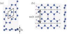
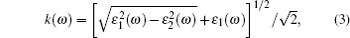
Compared with sp2 hybridization in the planar graphene, silicon shows a buckled surface with two sublattices not in the same plane because of its partial sp3 hybridization character. Based on phonon dispersion calculations, Cahangirov et al.[10] pointed out that that two-dimensional periodic low-buckled honeycomb structure of Si whose hexagonal lattice constant a, and low-buckled height b are 3.83 Å and 0.46 Å , respectively, is stable. The optimized atomic structure of Si hexagonal sheet by DFT-GGA is shown in Fig. 1(a), and the constants a and b are 3.83 Å and 0.47 Å , respectively. The values are in good agreement with those obtained by Cahangirov et al.[10]
 | Fig. 1. (a) Top and side views of the Si sheet with its unit cell indicated by a black parallelogram. The hexagonal lattice constant a, and the buckled height b are labeled. (b) The geometry structure of 7-ASiNR terminated with F atoms. The big blue and small gray balls represent Si and F atoms, respectively. The area between two black dashed lines represents the primitive periodic cell. |
The ASiNRs are constructed from the low-buckled silicon hexagonal sheet. Following the previous definition of the width for the nanoribbons, NA-ASiNRs are called the number of the dimmer lines across the ribbons width for the armchair edges. The optimized atomic structure and its side view of the F-terminated 7-ASiNR are shown in Fig. 1(b), and the primitive unit cells are indicated by the area between two black dashed lines.
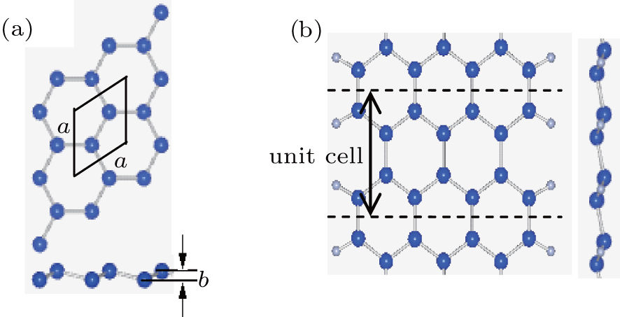
The charge density contours of F- and H-terminated 7-ASiNRs are shown in Fig. 2, respectively. Because of the larger electronegativity of 4.0 for the F atom than that of 1.9 for the Si atom, the maximum charge density values of 1.864 elections/Å 3 around the terminated F atoms are much higher than those of 0.150 elections/Å 3 around the Si atoms in the F-terminated 7-ASiNR, indicating that the charge distribution is very asymmetric. One can predict that electrons collect around F atoms, indicating a strong ionic bonding character. However, the Si– H bonds in Fig. 2(b) display a weak bonding feature, because of the slightly larger electronegativity of 2.1 for the H atom than that of 1.9 for the Si atom.
 | Fig. 2. Cross-sections along the ribbon of the charge density contours. (a) Buckled F-terminated 7-ASiNR and (b) buckled H-terminated 7ASiNR. Blue and red represent the lowest and the highest magnitude of the charge density. |
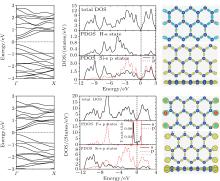
For analyzing the optical properties, the energy band, the total DOS and the projected density of states (PDOS) onto F, H, Si atoms for the F- and H-terminated 7-ASiNRs are shown in Fig. 3. In order to find the modification mechanism of the band gap, the charge density difference is calculated using the following equation: D = Dtotal − DF (or DH) − DSi, in which Dtotal is the total charge density of F- or H-terminated system; DF (or DH) and DSi are the charge densities after deleting all the Si atoms and F (or H) atoms in the system, respectively. It can be seen from the left panel in Fig. 3, the valence band maximum and the conduction band minimum locate along the Γ point, indicating that the F- and H-terminated 7-ASiNRs are direct band gap semiconductors. Moreover, the lowest conduction band shifts downward and the highest valence band shifts upward, which indicate the band gap of the F-terminated 7-ASiNR is narrower than that of the H-terminated one. From the charge density distribution in Fig. 3, it can be seen that F atoms is attributed to the interaction between non-bonding 2p valence electrons of F atoms and 3p valence electrons of the nearest Si atoms, i.e. the σ – π mixing effect, which is in good agreement with those obtained by Yang et al. The corresponding total DOS for F- and H-terminated 7-ASiNRs, as well as the PDOS onto F, H, Si atoms are shown in Fig. 3. By comparing the total DOS and the PDOS of F-terminated 7-ASiNR, the upper valence band and the conductor band between – 4 eV to 4 eV originates mainly from Si atoms especially their p orbital electrons, and the lower valence band from – 8 eV to – 11.5 eV is derived from the Si-3s states. The contribution of F-2p orbital electrons is primarily from – 5 eV to – 7 eV. However, the H atoms have a small contribution to the total DOS in H-terminated 7-ASiNR.
 | Fig. 3. Band structures (left panel), the total DOS, and PDOS on F (or H) and Si atoms (middle panel) and the charge density difference distributions (right panel, from top down, section, isosurface and side view. In sections, red and blue represent the maximum and the minimum charge density value) of H- (top panel) and F-terminated (bottom panel) 7-ASiNRs. |
Figure 4 shows the variations of the imaginary part of the dielectric function with photon energy for the H- and F-terminated 7-ASiNRs. It can be seen that firstly the variation of line shape of the dielectric function F-terminated 7-ASiNR with photon energy is the same as that of the H-terminated one. Secondly, the dielectric function of the F-terminated 7-ASiNR has an evident red shift, which is mainly attributed to the narrower band gap of the F atoms added to the system of 7-ASiNR. For instance, there are several dielectric peaks located at about 0.57, 1.71, 3.97, 4.88, 6.35, and 8.06 eV for the H-terminated 7-ASiNR, and 0.39, 1.57, 3.35, 3.94, 4.72, and 6.50 eV for the F-terminated 7-ASiNR. Combining the band structure and the PDOS of Si, H and F atoms in Fig. 3, we can see that the peaks at 0.57 eV and 0.39 eV correspond to the band gap values, and are caused mainly by the transitions of Si atoms s and p states electrons to the lowest conduction band for the H- and F-terminated 7-ASiNRs, respectively. The interband transitions below – 5 eV originate mainly from Si atoms s and p state electrons to the lowest conduction band, while the interband transitions above – 5 eV come from F atoms s states, Si atoms s states, and a small part of p states electrons. It can also be seen from Fig. 4 that the dielectric functions go to zero for both H- and F-terminated 7-ASiNRs in the high energy range. These properties indicate that the different terminated atoms of 7-ASiNRs affect mainly the optical properties in the low energy range.
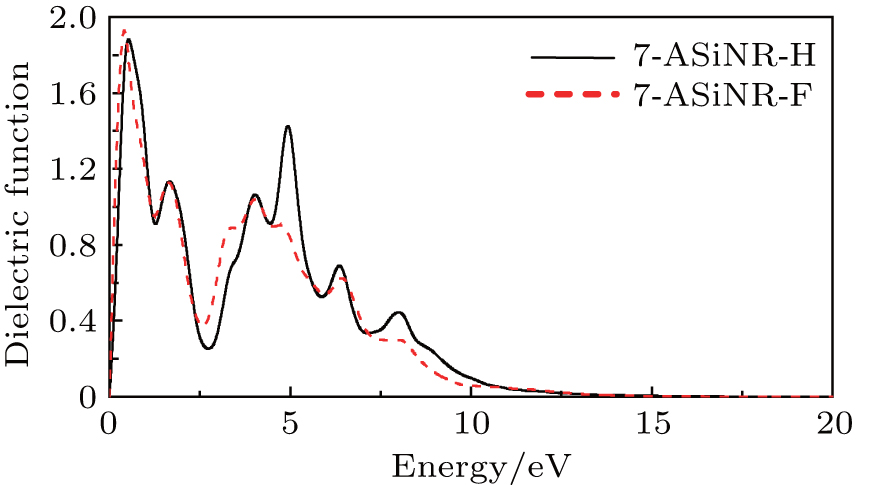 | Fig. 4. Variations of theoretically calculated imaginary part of the dielectric function with energy for H- and F-terminated 7-ASiNRs. The black solid and the red dashed lines indicate the dielectric functions of H- and F-terminated 7-ASiNRs, respectively. |
Figure 5 shows the curves of reflectivity of H- and F-terminated 7-ASiNRs versus energy in a range of 0 eV∼ 20 eV. There are six peaks in the low energy range located at 0.34, 1.59, 3.97, 5.11, 6.58, and 8.17 eV for the H-terminated system, and, 0.20, 1.58, 4.13, 4.92, 6.70, and 8.27 eV for F-terminated 7-ASiNRs. These peaks correspond to the peaks of the dielectric function in Fig. 4, which indicates that both of them have the same transition mechanism. The high photon-energy range (> 14 eV) is characterized by zero reflectivity. Moreover, even for the strongest reflectivity, the value is lower than 15%, and in the visible range (1.6 eV∼ 3.0 eV) the reflectivity is even lower.
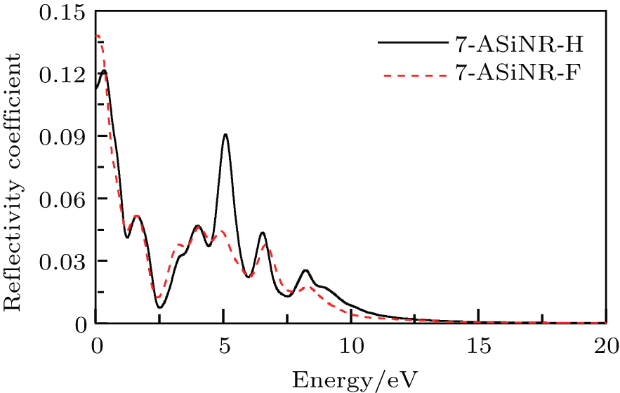 | Fig. 5. Variations of theoretically calculated reflectivity with energy for H- and F-terminated 7-ASiNRs. The black solid and the red dashed lines indicate the reflectivity values of H- and F-terminated 7-ASiNRs, respectively. |
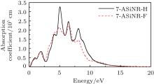
The absorption coefficient represents the attenuation rate when the optical wave passes through a medium in unit distance. Figure 6 presents the variations of absorption coefficient with energy for the H- and F-terminated 7-ASiNRs. It can be seen that the main absorption region is still located in the low energy area between 0 eV– 15 eV. In the high energy area, the absorption coefficient is almost zero. Taking into account all the reflectivity values of H- and F-terminated 7-ASiNRs in the visible range and the high energy area (> 15 eV), the systems can be seen as optically transparent materials.
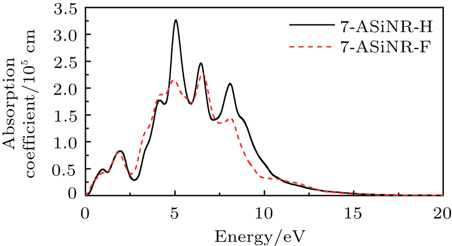 | Fig. 6. Variations of theoretically calculated absorption coefficient with energy for the H- and F-terminated 7-ASiNRs. The black solid and the red dashed lines indicate the absorption coefficients of H- and F-terminated 7-ASiNRs, respectively. |
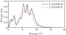
The energy loss function is an important factor for describing the energy loss of the electrons traversing in a material, and it is calculated and shown in Fig. 7. The peaks in the energy loss spectra represent the properties related to the plasma resonance, which is corresponding to the plasma frequency. The peaks of the energy loss are consistent with the trailing edges in the reflection spectra.[23] For instance, the peaks of the F-terminated 7-ASiNR are at about 0.91, 1.97, 4.33, 5.17, 6.70, and 8.27 eV corresponding to the abrupt reduction of reflection.
 | Fig. 7. Variations of energy-loss coefficient with energy for (a) H- and F-terminated 7-ASiNRs and (b) H- and F-terminated 7-ASiNRs. The black solid and red dashed lines denote the energy-loss coefficient of F- and H-terminated 7-ASiNRs, respectively. |
In this work, the optical properties of the H- and F-terminated 7-ASiNRs are systematically investigated by using the first-principles PAW potential within the DFT framework under GGA. The following conclusions are obtained.
(i) The line shape of the dielectric function for the F-terminated 7-ASiNR is the same as that of H-terminated one and has an evident red shift, which is mainly attributed to the narrower band gap because of the interaction between non-bonding 2p valence electrons of F atoms and 3p valence electrons of the nearest Si atoms.
(ii) These peaks of reflectivity correspond to those of the dielectric function. The high photon-energy range (> 14 eV) is characterized by zero reflectivity. The strongest reflectivity is lower than 15%, and in the visible range (1.6 eV∼ 3.0 eV) which is even lower.
(iii) The peaks in the energy loss spectra represent the characteristic associated with the plasma resonance and the corresponding frequency is the so called plasma frequency. The peaks of the energy loss correspond to the trailing edges in the reflection spectra.
In this paper, the simulation results of these properties show that the different terminated atoms of 7-ASiNRs affect mainly the optical properties in the low energy range and very weakly in high energy range. Because of the rich optical properties, F- or H terminated 7-ASINRs could be a potential candidate for a short– wavelength photoelectric nanodevice.
| 1 |
|
| 2 |
|
| 3 |
|
| 4 |
|
| 5 |
|
| 6 |
|
| 7 |
|
| 8 |
|
| 9 |
|
| 10 |
|
| 11 |
|
| 12 |
|
| 13 |
|
| 14 |
|
| 15 |
|
| 16 |
|
| 17 |
|
| 18 |
|
| 19 |
|
| 20 |
|
| 21 |
|
| 22 |
|
| 23 |
|