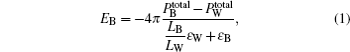
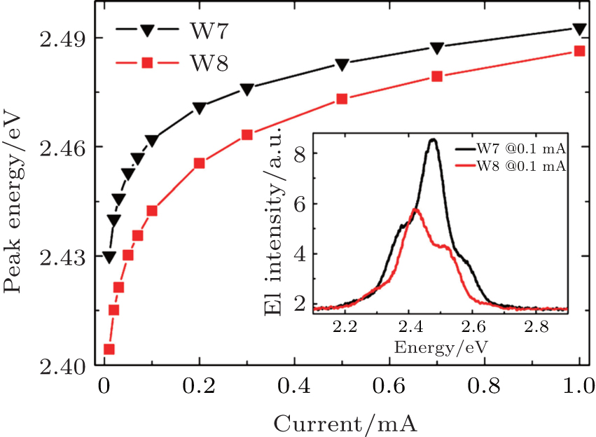
3. Results and discussionFigure 1 indicates the blueshifts of the EL peak energy of LEDs W7 and W8 with DC injection current increasing from 0.01 mA to 1 mA at room temperature (RT).
It can be seen that the blueshift amount of W8 is larger than that of W7. For instance, when the injection current increases from 0.01 mA to 1 mA, the peak energy of W8 increases about 82 meV, while that of W7 increases about 63 meV. The larger amount of blueshift with increasing current can be seen as an indication of the existence of a stronger quantum confined Stark effect (QCSE) in LED W8. It is induced by the enhanced piezoelectric polarization effect when the InGaN well layers become thicker. The typical RT EL spectra of LEDs W7 and W8 at injection DC I = 0.1 mA are also shown in the inset in Fig. 1. Compared with LED W7 with a peak emission energy of 2.46 eV (about 504 nm), the peak energy of W8 decreases to 2.44 eV (about 508 nm) and the EL intensity of W8 becomes smaller too. These changes may be attributed to the weaker quantum confinement effect and stronger QCSE due to the increase of QW layer thickness in LED W8.
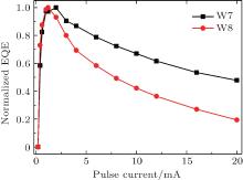
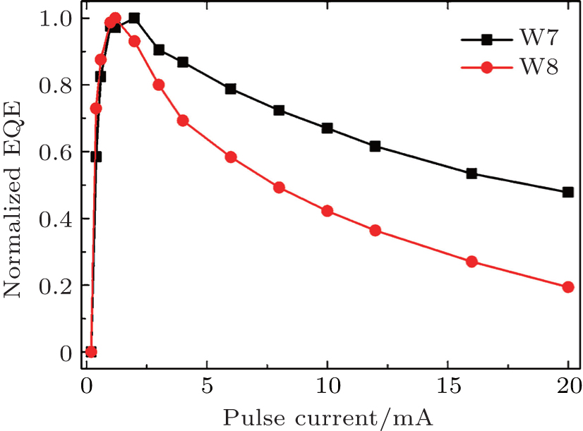
The EQE droop curves of LEDs W7 and W8 are normalized and plotted in Fig. 2. It is found that the droop curve of W8 decays faster than that of W7 as injection current increases. For example, the amount of efficiency droop for LED W8 from the highest EQE value at 1.2 mA to the lowest value at 20 mA is almost 80%, which is significantly larger than that for LED W7, i.e., the LED with thicker QW layers exhibits a more severe droop behavior. In the InGaN/GaN MQW structure, the piezoelectric polarization charges at the heterointerfaces, caused by the lattice mismatch between the InGaN wells and GaN barriers, can slope the conduction bands upward from the n side to the p side and form triangular potential barriers for carriers in GaN layers in the MQW active region.[13] The electric field EB in GaN barrier layers can be expressed as follows:[17]
where Ptotal, ε , and L represent the electric polarization, dielectric constant, and layer thickness, respectively. Both subscripts of W and B represent well and barrier layers, respectively. According to Eq. (1), the electric field EB becomes larger when the well thickness LW increases, i.e., the slope of the energy band in the GaN barrier layer becomes larger when the In- GaN well layers become thicker. For the LEDs with thicker well layers, the sloped triangular potential barriers in the GaN layer for both electrons and holes are enhanced, and hinder the carriers to pass through the GaN barrier layers, thereby requiring an increased bias to drive sufficient current through MQW active regions.[14] As a result, the conduction band on the n side may become higher in the thick-well MQW. To support this deduction, the calculated conduction band diagram of In- GaN/GaN MQW region at 10 mA forward current is plotted in Fig. 3.
Obviously, first the conduction band on the n side is higher than that on the p side for both samples. Second, the conduction band differences between n and p sides are 42 meV and 111 meV for W7 and W8, respectively. In other words, under the same forward current condition, for LED W7, the conduction band on the n side is lifted and becomes much higher than that on the p side for LED W8 with thicker well layers. The higher conduction band on the n side makes the electrons energetically favorable for escaping to the p side without being captured by InGaN QWs, thus leading to a large electron leakage current. Consequently, the droop behavior becomes more significant for the thick-well MQW LED W8.
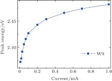
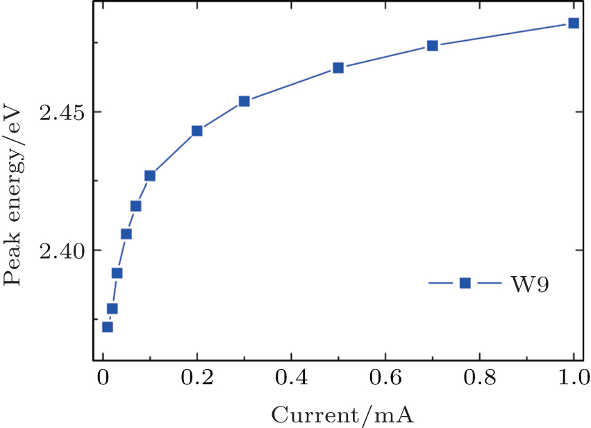
To further check our deduction about the influence of well layer thickness on the droop behavior, LED W9 with increased QW thickness of 3.4 nm is additionally investigated. To check the polarization effect in W9 first, the blueshift of the EL peak energy of LED W9 with increasing injection current is shown in Fig. 4.
Compared with the scenario in Fig. 1, in general the peak emission energy of W9 is smaller than those of W7 and W8 due to the lesser quantum confinement effect and stronger QCSE. Furthermore, the blueshift amount of W9 becomes about 109 meV, which is larger than those of W7 and W8, when the injection current increases from 0.01 mA to 1 mA. This indicates that in LED W9 with increased QW thickness the polarization effect or the QCSE is enhanced.
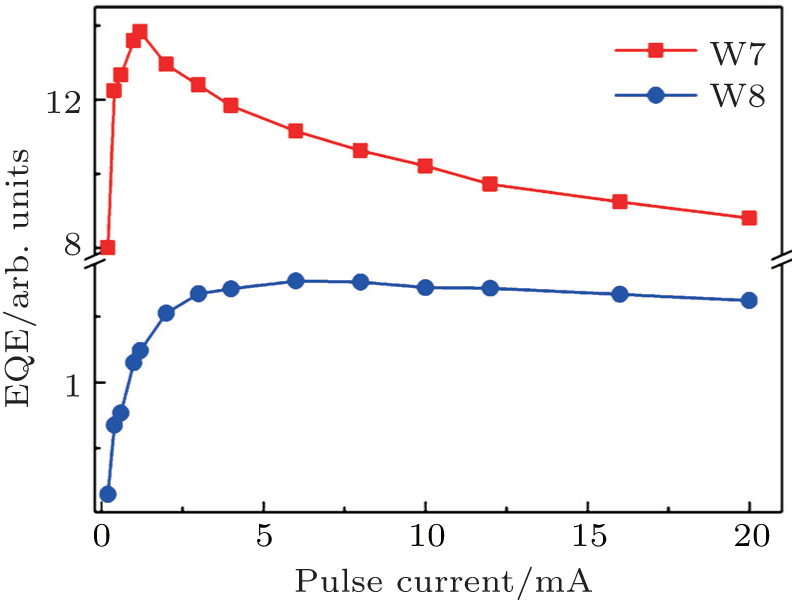
The EQE droop curves for both LEDs W8 and W9, measured under PC mode, are compared and depicted in Fig. 5. It is interesting to note that a very little EQE droop (less than 10%) is observed for W9 in the current range up to as high as 20 mA, although the polarization effect in LED W9 is the strongest in all 3 LEDs due to the thickest InGaN well layer. This result implies that the enhanced polarization effect may have less contribution to the aggravation of efficiency droop for LED W9, and additional physical mechanisms should be taken into account for the significant reduction of efficiency droop.
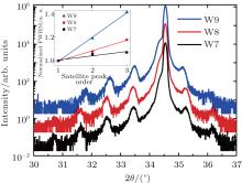
In addition, it is apparent that in Fig. 5 the EQE values of W9 are remarkably smaller than those of W8, which may be ascribed to the enhanced QCSE induced by the increased well layer thickness. We are also aware that the material quality of InGaN/GaN MQW LEDs may be influenced by the increased QW thickness. Therefore, the (0002) ω – 2θ scan XRD curves for all samples are measured and depicted in Fig. 6.
It can be seen in Fig. 6 that W7 has 4 well-distinguished satellite peaks of superlattice (SL) structure, but only 3 satellite peaks can be distinctly observed for W9. As is well known, the full widths at half maximum (FWHMs) of satellite peaks will be broadened if the interface roughness of the SL structure exists, and for the MQW structures the number of observed satellite peaks will be reduced by the rougher interface. If the interface roughness is described by a Gaussian distribution function with standard deviation, the FWHM of the n-th satellite peak will be expressed as[18]

where n is the order of satellite peak, Λ is the period length, Δ θ M is the angle distance between adjacent satellite peaks, and σ /Λ is the interface roughness, W0 and Wn are the FWHM values of 0-th and n-th order satellite peaks, respectively. The inset shows the relationship between the satellite peak FWHM and the peak order for the MQW structures of W7, W8, and W9, denoted by black squares, red circles, and blue triangles, respectively. According to Eq. (2), LED W9 has the roughest interfaces, since the slope value of W9 is the largest in the values of all three samples as shown in the inset of Fig. 6. In fact, if the In content increases to 20%, as in our samples, the critical thickness of InGaN QW is about 3.5 nm.[19] This value is almost equal to the InGaN well layer thickness of W9. As the QW thickness approaches to a critical thickness, the stress induced by a lattice mismatch between InGaN wells and GaN barriers becomes larger, and then the strain relaxation may occur, generating more dislocations and roughing the interface. Therefore, the MQW quality of W9 may deteriorate seriously, i.e., more defects may appear in the MQW active region of W9. When a large number of defects or dislocations acting as non-radiative recombination centers exist in the MQW active regions, more injected carriers are inclined to be captured by the increased non-radiative recombination centers, giving rising to the remarkable reduction of absolute EQE as shown in Fig. 5.
Furthermore, in Figs. 2 and 5 it is worthwhile noting that there are two different types of droop curves as observed. For instance, for LED W9, the EQE curve tends to have a slow rise, and it decays also very slowly in a nearly constant low rate with increasing injection current, while for both LEDs W7 and W8, the EQE curves each exhibit a faster rise at lower currents, followed by a rapid decay, and afterwards approach the lower decay rates similar to what is observed for W9. We believe such different droop behaviors may be related to the so-called carrier localization and delocalization effects in the InGaN QWs.[9, 10]
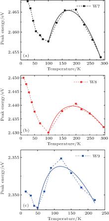
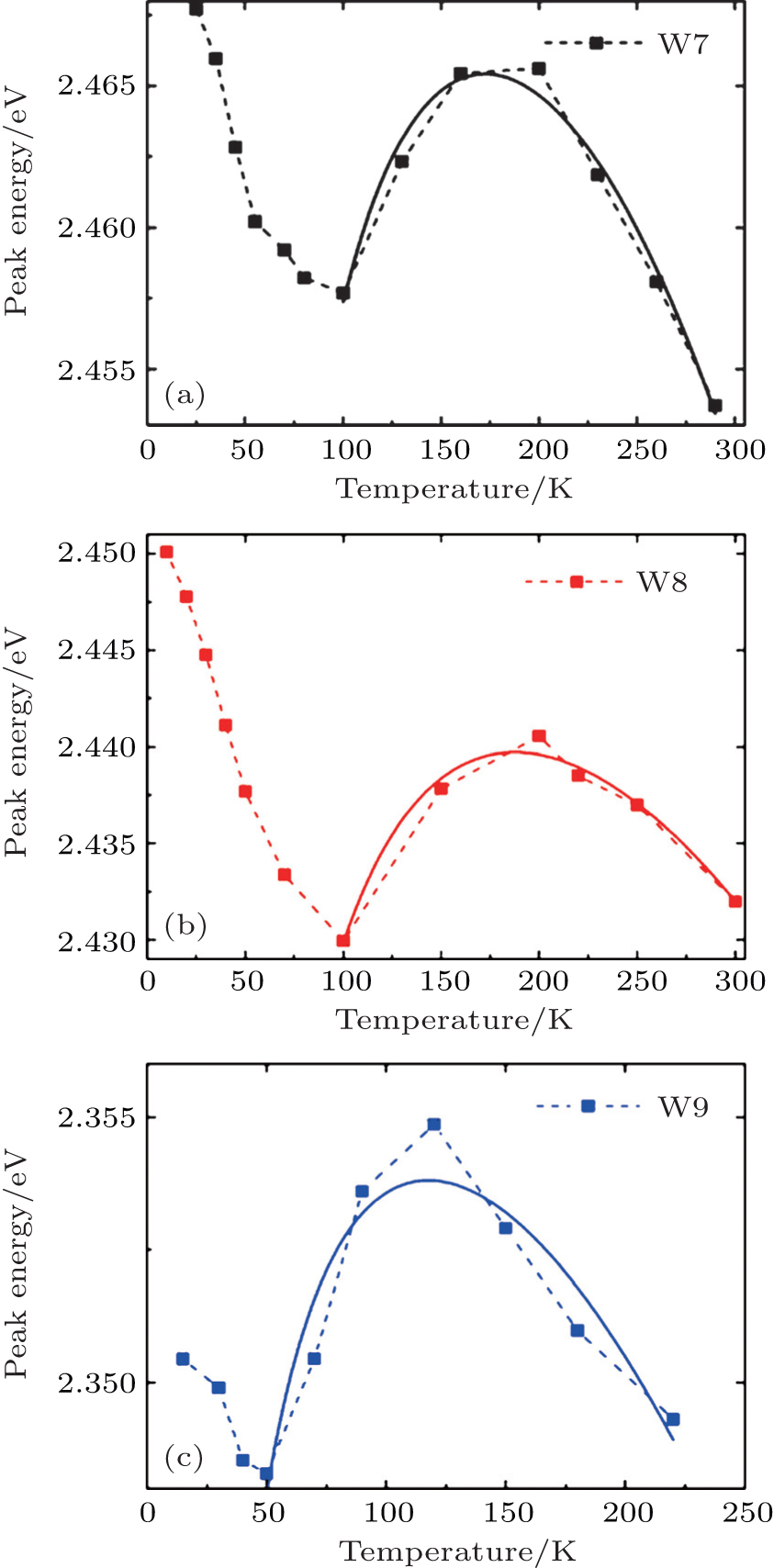
To investigate the localization effect first, the PL peak energy as a function of temperature is plotted in Fig. 7. An anomalous S-shape shift with increasing temperature is observed for each of all three studied samples. The S-shape behavior is a fingerprint of the existence of localization effect, where the blueshift of the emission peak with increasing temperature is caused by the process in which the thermally excited carriers migrate out from the deep localized potential minima and populate the higher energy levels in the shallow localization states.[20] It is observed that in W9 the blueshift happens at very low temperature (about 50 K) while for the other two LEDs it happens at about 100 K. It means that in W9, carriers need less thermal energy to escape from the localized potential minima, i.e., the confinement energy of localization states in W9 is comparatively smaller than those in W7 and W8 on average.
To make a more quantitative analysis, a band-tail model can be used to describe the localization states in InGaN QWs where the band-tail states are treated as localization states. In InGaN QWs, band tail states can appear in the electron energy diagram as a result of disorders in the crystalline structure, introduced by either QW thickness fluctuations or nonuniformity of alloy composition (e.g., indium-rich clusters in InGaN). The tail states which provide the energy levels for confined localized carriers are statistically distributed below the band edge.[21] It is noted that these band-tail states are suitable to provide efficient luminescence centers because these states can confine electrons and holes at the same sites, and the relevant matrix elements for optical transition can be as large as in the case of free carriers. As suggested by Eliseev et al., in the band-tail model, the temperature-dependent emission peak energy can be given by the following expression:[22]
where E0(0) is the band-gap energy at 0 K, T is the temperature, kB is the Boltzmann constant, α and β are known as Varshni’ s fitting parameters. The third term on the right-hand side in Eq. (3) comes from the carrier localization effect, in which σ indicates the extent of localization effect. Originally, in the band-tail model, σ is defined as an energy parameter of the distribution of the band-tail states below the nominal band edge.[21] The distribution of density of band-tail states is approximately considered as a Gaussian function of energy E. The density of states (DOS) functions of electrons and holes ρ e, h(E) in the conduction and valence bands are
where σ e and σ h are the dispersion of electron and hole Gaussian distribution, respectively. Thus, the parameter σ describes the broadening effect and the shape of the band tail. It implies that the larger the σ value, the more deeply the tails extends into the nominally forbidden band, i.e., a large value of σ means a stronger localization effect.
For comparison, the experimental data and the fitting curves based on Eq. (3) are shown in Fig. 7 together. The fitted values of σ are 18.1 meV, 17.6 meV, and 8.0 meV for LEDs W7, W8, and W9, respectively. It can be seen that the σ value of LED W9 is much smaller than those of the other two LEDs, which demonstrates that the localization effect is much weaker in W9, while it becomes stronger in both W7 and W8. The differences in localization effect between thick and thin QWs may originate from the accumulation of the strain energy in InGaN QW layers, which has been analyzed in more detail elsewhere.[23]
According to our analysis about the localization effect, by combining with the XRD results, the different droop behaviors can be explained as follows. For LEDs W7 and W8 with better MQW material quality and less non-radiative recombination centers, at low currents, a strong localization effect causes more carriers to be captured by the deep localization states and the carriers over there recombine radiatively mainly, leading to a fast rise of EQE curve with increasing current and a high peak EQE value. As the injection current increases continuously, more and more injection carriers cannot be captured by the localization states due to the state-filling effect, namely, the delocalization effect occurs. One should keep in mind that the delocalization effect itself does not quench the radiative recombination efficiency. However, these released carriers are either very susceptible to the defects outside the localization states and then recombine non-radiatively by the SRH processes, or more inclined to overflow to the p-GaN layer.[7] It means, therefore, that the delocalized carriers will have less contribution to the luminescence, leading to a rapid decrease of EQE with increasing injection current. With increasing current further, since most of the injected carriers cannot be captured by the localization states any more, the influence of delocalization effect becomes less significant. Consequently, the droop rate decreases gradually for the further increase of current. However, for LED W9, the localization effect is much weak and the non-radiative recombination process is strong, thus it is very hard for carriers to be captured by the shallow localization states and recombine radiatively, causing a slow rise of EQE curve with increasing injection current. Since the localization effect is the weakest, a large portion of carriers cannot be trapped in the localized states. Correspondingly, the delocalization effect induced by the state-filling effect is less significant, giving rise to a slower decay of EQE curve with continuously increasing injection current. It should be mentioned that a reduction of emission efficiency for each of all LEDs at very high current (e.g., larger than 15 mA) may also originate from other physical factors, such as Auger recombination which is proportional to the third power of carrier density in QWs.[11]
Based on the aforementioned analysis, there is no monotonic variation of efficiency droop when the InGaN well layer thickness increases for greenMQWLED. When the well layer is very thin, with increasing well thickness, the efficiency droop becomes more severe due to the enhanced polarization effect. As the thickness increases further, more severe electron leakage may occur at high currents due to the much stronger polarization effect. However, since the enhanced non-radiative SRH process, induced by both lattice relaxation and weak localization effect, can suppress the radiative recombination in InGaN QW at a relatively wide current range, the influence of electron leakage at high currents on the radiative recombination, i.e., light emission, becomes less significant.[24] In other words, the SRH non-radiative recombination is still stronger than the radiative recombination even beyond the point where the electron-leakage mechanism becomes dominant at relative high currents and the radiative recombination may never become the dominant recombination mechanism, resulting in the lower peak efficiency and the absence of a significant efficiency droop for LED W9. Since the absolute luminescence efficiency of LED W9 diminishes seriously, it cannot meet the requirement of the practical LED applications. On the other hand, the reduction of polarization effect can benefit both the enhancement of luminescence efficiency and the alleviation of efficiency droop, which thus may be regarded as a practical consideration for designing high-brightness light emitting devices.


 , Jiang De-Sheng