


Comparative research on the optical properties of three surface patterning ZnO ordered arrays
[Hou Kai, Zhu Ya-Bin† , Qiao Lu]
, Qiao Lu]
|
|


†Corresponding author. E-mail: ybzhu@bjtu.edu.cn
We fabricate three surface patterning zinc oxide (ZnO) ordered arrays on glass substrates by using nanosphere lithography technique and dc magnetron sputtering technique. The crescent, tube and honeycomb surface morphologies of the samples are observed by scanning electron microscopy. The transmittance, fluorescence and confocal Raman spectra of the sample are measured. Obviously, when the angle between the plume and the substrate is 90°, the honeycomb arrays have a better transmission. Additionally, the PL intensity of honeycomb arrays is superior. With the increasing of the angle between the substrate and the sputtering plume, the fluorescence peak shows blue shift. The Raman peak located at 438 cm− 1 belongs to ZnO E2 (high) mode, which corresponds to the characteristic band of the hexagonal wurtzite phase. The tube arrays have the best Raman spectrum intensity.
Surface patterns on various substrates have attracted intensive attention in the development of photonic crystal, [1, 2] resonators, [3, 4] storage media, [5] photocatalyst, [6] nanoemitter, [7] and so on. Surface patterns (for example, nanotubes, nanorods, nanowires, nanobelts, and nano-flower-like structure[4, 8]) can be prepared by using either expensive methods including focused beam ion (FBI)[9] and electron beam lithography (EBL)[10] or the low-cost processes including nanosphere lithography (NSL)[11] and nano-imprinting.[12] Therein, the nanosphere lithography is more extensively used because of the simple and practicable operation following three steps. Firstly, colloidal sphere templates are prepared on substrates by self-assembly process; secondly, aimed metal or compounds are deposited on the templates and substrates by using evaporation, pulsed laser deposition or hydrothermal method; thirdly, ordered arrays can be obtained by removing the colloidal spheres templates through using organic solvents (e.g. chloroform) or burning process. With these three approaches, Retsch et al. prepared Au nano-crescent resonators; [3] Li et al. reported that they obtained more complex hexagonal-close-packed, hierarchical amorphous titanium dioxide (TiO2) to enhance photocatalytic activity; [6] Sun et al. reported gold (Au) nanoparticles hexagonally arranged on ITO glass substrate.[13] Gwinner et al. fabricated an ordered array Au split-ring resonator.[14] Obviously, it is important to fabricate the various surface pattern ordered arrays for nanodevices.
As is well known, zinc oxide (ZnO) is a wide direct band-gap (∼ 3.37 eV) semiconductor material and its high exciton binding energy is about 60 meV. It can be widely used in optoelectronic applications, such as ultraviolet (UV) light-emitting diodes, [15] UV detectors, [16] nonlinear optics, [17] etc. In recent decades, there were a number of research studies on nanostructured ZnO because of natural faceting, large surface-to-volume ratio, and quantum size effects different from those of ordinary materials. Guo et al. have synthesized ZnO nanoflowers and investigated their wettabilities and photocatalytic properties.[18] Huang et al. have fabricated nano-scale honeycomb broadband anti-reflection structure to enhance the efficiency of silicon solar cells.[19] Peng et al. have prepared low-dimensional nanostructure ultraviolet photodetectors.[20] In our previous work, we have reported that ZnO honeycomb arrays[21, 22] were fabricated by using polystyrene sphere (PS) templates and magnetron sputtering method and studied the optical properties of ZnO honeycomb ordered arrays. However, there is a lack of a suitable simple technique to fabricate other shaped surface patterns.
In this paper, we obtain three surface patterns, i.e., crescent, tube and honeycomb, by simply adjusting the angle between the substrate and the sputtering plume, and comparatively study the optical properties of three ZnO surface patterns.
PS with 1000 nm in diameter was used to prepare templates on normal substrates by drift method.[21, 22] The prepared templates were placed on the substrate holder with respect to sputtering plume at the angles of 0° , 30° , and 90° in a vacuum dc magnetron sputtering deposition system, respectively, as shown in Fig. 1. Zn target purity was 99.99%, high-purity argon gas (99.9999%), and high-purity argon oxygen (99.9999%) were introduced into the chamber with the gas ratio 2:1. The base pressure was 5 × 10− 4 Pa, and in the whole deposition process the working pressure maintained 4 Pa. The sputtering current was 200 mA with a sputtering voltage of 320 V, and the substrate temperature was kept at 200 ° C. All the samples, each with 300 nm in thickness, are obtained after 60-min sputtering. Finally, the samples were annealed at 400 ° C in a muffle furnace for 2 h after ultrasonic washing in chloroform for 5 min to remove the PS spheres.
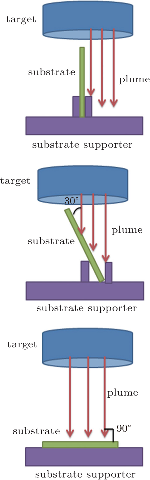 | Fig. 1. Schematic diagram of sputtering target and substrate. |
Surface morphologies of PS templates and ZnO arrays were observed by Zeiss SUPRA 55-type field emission scanning electron microscopy (SEM) and energy dispersive x-ray analysis (EDX); Avantes standard spectrometer 2048 × 14 using a light transmittance was used to measure the transmittance of ZnO thin film arrays; F-4600 fluorescence spectrometer was used to measure the fluorescence spectra of ZnO arrays; Raman spectra of samples were measured by LabRam HR800 confocal microscopy.
Figure 2 is an SEM image of monolayer PS template with a size of 4.9 μ m× 3.2 μ m. The periodic, neat, hexagonal array consists of spheres with a diameter of 1000 nm. The PSs show quasi-point contact to each other. A slight deformation may be attributed to the deposition of gold for electric conduction required by the SEM observation.
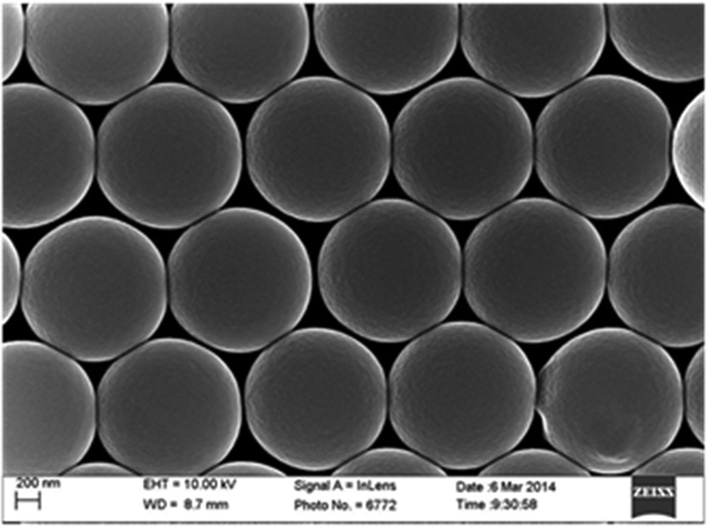 | Fig. 2. SEM image of polystyrene spheres with a diameter of 1000 nm. |
Figure 3 shows the surface microscopy images of samples fabricated at angles between the plume and the substrate of 0° (a), 30° (b), and 90° (c). The surface microscopy image of ZnO array fabricated at the angle between the plume and the substrate of 0° is shown in Fig. 3(a) (top-view), the inset shows a side-view ZnO tube with 1 μ m in length. Figure 3(a) shows uniformly and neatly arranged ZnO array in a size of 21.3 μ m× 20.4 μ m, in which the ZnO circular ring is 1000 nm in diameter.
 | Fig. 3. SEM images of sample prepared at the angles between substrate and plume of 0° (a), 30° (b), and 90° (c). |
Figure 3(b) shows the top view of ZnO hexagonal arrangement of half-moon shape, the long axis of half-moon is about 637 nm and the short axis is about 455 nm. The half-moon ZnO array obtained does not follow the process of fabricating nano-crescent arrays described by Lei et al.[23] The mechanism is complicated, which needs further studying. In this paper, we focus on the shape of ZnO arrays and the optical properties.
The surface microscopy images of ZnO array fabricated at the angle between the plume and the substrate 90° is shown in Fig. 3(c). Figure 3(c) shows triangle-shaped ZnO, uniform and orderly hexagonal arrangement in a size of 21.3 μ m× 20.0 μ m. The triangle side length is 268.5 nm that is obtained from the equation,

where h is the height of triangle, and D is the diameter of PS colloidal sphere.
Figure 4 shows an energy dispersive analysis (EDX), indicating that the main elements of the area are oxygen (O), silicon (Si), and zinc (Zn). The Si peak is probably from the normal glass substrate, and the carbon (C) peak is due to the evaporation of C, for ZnO arrays are better conductive before the observation of the SEM.
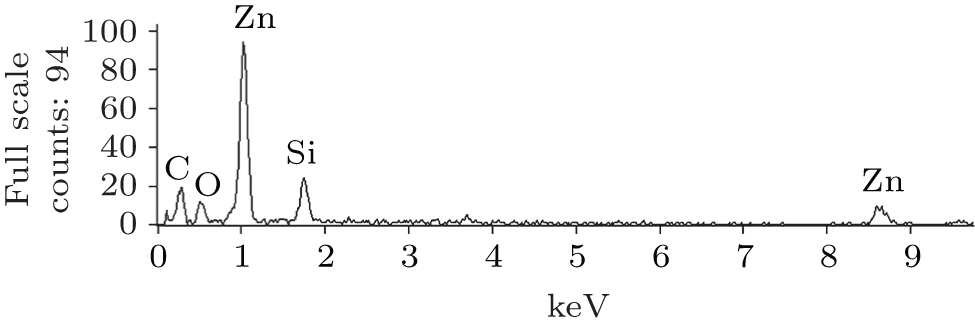 | Fig. 4. EDX spectrum of sample. |
Figure 5 shows the transmission spectra of ZnO arrays fabricated at the angles between the plume and the substrate of 0° , 30° , and 90° , respectively. There is one obvious absorption peak at 354 nm which is near the band gap of ZnO in each of the crescent, tube and honeycomb surface pattern transmission spectra. Obviously, when the angle between the plume and the substrate is 90° , the honeycomb arrays have a better transmission. The occupied area of ZnO is larger than that of the others on substrate.
 | Fig. 5. Transmission spectra of ZnO arrays at the angle between substrate and plume of 0° , 30° , and 90° . |
The transmission spectra can be obtained by solving the Maxwell equations. Mie theory is used for strict mathematical isotropic spherical particles of light absorption and scattering analytical solution. Discrete dipole approximation (DDA) calculation can simulate any shape of particle. Our previous work (see Refs. [21] and [22]) described the theoretical transmission spectrum of honeycomb arrays by the DDA method. Our present study is to simulate the transmission spectrum of crescent and tube arrays.
Figure 6 shows the fluorescence spectra of ZnO arrays fabricated at the angles between the plume and the substrate at 0° , 30° , and 90° , respectively. Excitation laser wavelength is 320 nm, and the measurement range is from 340 nm to 625 nm. As can be seen from the figure, ZnO films have luminescent peaks at 404 nm, 401 nm, and 397 nm for the crescent, tube and honeycomb surface pattern, respectively. With the increase of the angle between the plume and the substrate, the fluorescence emission peaks become blue-shifted. Generally, it is believed that the emission peaks are generated mainly by free-exciton interband transitions. The inset shows that the luminescent peak of ZnO thin film is at 378 nm. This phenomenon can be attributed to the quantum size effect, with the increase of the angle between the substrate and the sputtering plume, the size of nanoclusters structure of ZnO becomes larger, causing the fluorescence peak to be blue-shifted. Additionally, the PL intensity of tube arrays is superior.
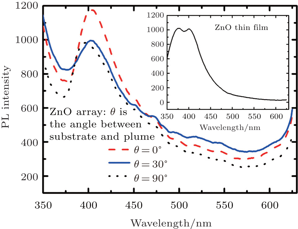 | Fig. 6. Fluorescence spectra of ZnO arrays, and the fluorescence spectrum of ZnO film (in the inset). |
The confocal microscopy Raman curves are measured when the incident laser wavelength is 632 nm as shown in Fig. 7. The Raman peak located at the 438 cm− 1 belongs to the ZnO E2 (high) mode, and with the variation of the sputtering angle, the Raman peak does not have significant shifts and the band line is not significantly widened nor shifted, which is not in accordance with the results reported by Li and Chen.[24] It is obviously observed that the tube arrays have the best Raman spectrum intensity.
 | Fig. 7. Raman spectra of ZnO arrays. |
In this work, it is verified that crescent, tube and honeycomb ZnO surface patterns can be obtained by only changing the angle between the substrate and sputtering plume into 0° , 30° , and 90° , respectively. The technology is related to low-cost magnetron sputtering, nanosphere lithography technique, ultrasonic washing and annealing in a muffle furnace. The SEM images are observed and the transmittance, fluorescence and confocal Raman spectra of the sample are measured. When the angle between the plume and the substrate is 90° , the honeycomb arrays have a better transmission. Additionally, the PL intensity of tube arrays is superior. The tube arrays have the best Raman spectrum intensity. With the increase of the angle between the substrate and sputtering plume, the fluorescence peak shows blue shift.
The authors thank Prof. Qiu Xiang-Gang of Institute of Physics, Chinese Academy of Sciences for kindly providing us with dc magnetron sputtering equipment and Avantes standard spectrometer 2048×14.
| 1 |
|
| 2 |
|
| 3 |
|
| 4 |
|
| 5 |
|
| 6 |
|
| 7 |
|
| 8 |
|
| 9 |
|
| 10 |
|
| 11 |
|
| 12 |
|
| 13 |
|
| 14 |
|
| 15 |
|
| 16 |
|
| 17 |
|
| 18 |
|
| 19 |
|
| 20 |
|
| 21 |
|
| 22 |
|
| 23 |
|
| 24 |
|