


Study of Nb/Nb xSi1− x/Nb Josephson junction arrays
[Cao Wen-Hui† , Li Jin-Jin‡, Zhong Yuan, He Qing]
, Li Jin-Jin‡, Zhong Yuan, He Qing]
|
|


†Corresponding author. E-mail: caowh@nim.ac.cn
‡Corresponding author. E-mail: jinjinli@nim.ac.cn
*Project supported by the National Key Technology Research and Development Program of the Ministry of Science and Technology of China (Grant No. 2011BAK15B00), the Young Scientists Fund of the National Natural Science Foundation of China (Grant No. 61401418), and the Basic Research Foundation of National Institute of Metrology of China (Grant No. 20-AKY1415).
Owing to the adjustable characteristics and superior etching properties of co-sputtered Nb xSi1 − x film, we are trying to fabricate Nb/Nb xSi1 − x/Nb Josephson junction arrays for voltage standard. It is important to find the suitable Nb xSi1 − x barrier for the junctions. Josephson junctions with different barrier content are fabricated. Current–voltage characteristics are measured and analyzed. It is demonstrated in this paper that critical current can be adjusted by using different barrier content and thickness. Shapiro steps of five hundred junctions in series are observed.
The non-hysteretic type Josephson junction arrays consisting of hundreds of thousand junctions are the basis of alternating current (AC) Josephson voltage standard.[1, 2] With non-hysteretic current– voltage (I– V) curve and large critical current, the superconductor– normal metal-superconductor (SNS) junction devices are capable of realizing stable voltage steps and good noise immunity. Nb and NbN are the most mature and commonly used superconductor materials for the SNS junction devices, while PdAu, [3] MoSi2, [4] TiNx, [5] and NbxSi1− x[6] are usually chosen as the barrier materials. The advantages of the Nb/NbxSi1− x/Nb Josephson junction include: 1) the junction parameters, namely electrical resistivity and critical current density, can be easily tuned by changing the composition and thickness of NbxSi1− x barrier; 2) both NbxSi1− x and Nb layer can be etched simultaneously by using one etching recipe, which is very convenient for the junction fabrication.[7] National Institute of Standards and Technology (NIST) has already demonstrated wafer-scale uniform and reproducible 10-V programmable Josephson voltage standard chips which can operate at about 18 GHz with using NbxSi1− x as barrier material.[6] 20-V Josephson junction arrays with NbxSi1− x barrier working at 70 GHz have been successfully fabricated by Physikalisch-Technische Bundesanstalt(PTB).[8] 1-V Josephson arbitrary waveform synthesizer was also demonstrated by NIST[9] and PTB[10] separately.
Recently we just started to fabricate Nb/NbxSi1− x/Nb Josephson junctions.[11] The content of NbxSi1− x barrier can be easily adjusted by using different Nb and Si sputtering powers separately. Josephson junctions with different properties have been fabricated and tested. Shapiro steps for junction arrays are also observed. The fabrication procedure and measurement results will be discussed in this paper.
According to the resistively– capacitively shunted junction (RSCJ) model, the damping properties of Josephson junction are determined by the McCumber parameter β c = 2π IcR2C/Φ 0, where C is the capacitance of the junction geometry, R is the linear damping resistance, Φ 0 is the quantum flux, and Ic is the junction critical current. When β c < 1, the junction is overdamped and the current– voltage (I– V) curve of the junction is non-hysteretic, that is, the junction voltage is a single-valued function of the junction current.[12] By adjusting the NbxSi1− x content of Nb/NbxSi1− x/Nb Josephson junction, Ic and R can be tuned and the junction can be non-hysteretic. If a junction is driven at frequency f, then its I– V curve will develop regions of constant voltage at the value nh f/2e, where n is an integer, e is the elementary charge, and h is the Planck constant. If I– V curve of the junction is non-hysteretic, then the voltage steps can be exactly selected by using bias current. The junction arrays used in programmable voltage standard often work at dozens of gigahertz corresponding to a voltage step of dozens of micro-volt for one junction. So integrating more junctions in an array and increasing the working frequency are conducive to voltage standard which is 1 V or 10 V.[3, 6]
In order to study Josephson junctions with different areas, junction arrays containing square junctions with different sizes are designed on the chip. For the microwave transmission line, junction arrays containing 500 junctions are arranged in a straight line within the co-planar waveguide (CPW). The CPW transmission line has tapered impedance such that each junction in the transmission line can receive nearly uniform microwave current. The impedance of the 8 mm length CPW is started at 50 Ω and ended at 44 Ω . There are also photolithography test patterns and endpoint areas for etching designed on the chip.
Nb/NbxSi1− x/Nb sandwich layers were deposited on 2- inch (1 inch = 2.54 cm) oxidized silicon (100) substrates by direct current (DC) magnetron sputtering at a base pressure of 1 × 10− 8 Torr (1 Torr = 1.33322 × 10² Pa). The substrate holder was rotated during the deposition in order to improve the uniformity of the films. There were three 3-inch targets in the chamber, i.e., one silicon target and two Nb targets. The Nb films were deposited with a sputtering power of 500 W in 5.1-mTorr Ar atmosphere, corresponding to a deposition rate of 0.75 nm/s. This power could not let the target become too hot and the deposition rate was also moderate. Nb film with a very small compressive stress of about 100 MPa and critical temperature of 9.1 K was obtained. The NbxSi1− x film was co-sputtered by using Nb and Si targets, with Si sputtering power fixed at 248 W and Nb sputtering power changed from 80 W to 50 W. By measuring the Si deposition rate and Nb deposition rate separately, the co-sputtering deposition rate is known. Through controlling the sputtering time, the barrier thickness could be known. The deposition rate for the Nb target at 50 W was about 0.033 nm/s, corresponding to a change of 0.003 nm per 5 W. It was a very small change compared with the Si deposition rate of 0.15 nm/s at 248 W. So a common rate of 0.18 nm/s for calculating the barrier thickness was used. During deposition of the tri-layer films, the substrate was backside cooled by flowing water. The temperature of the wafer was about 40 ° C after the tri-layer deposition.
After deposition of the sandwich layers, Nb/NbxSi1− x/Nb Josephson junction devices were fabricated by sequentially using standard photo lithography with a resolution of 1 μ m, reactive ion etching (RIE), plasma enhanced chemical vapour deposition (PECVD) and lift-off process. The junction area was defined by using an inductively-coupled-plasma (ICP) deep reactive-ion etching (RIE) with a mixture of etch (SF6) and passivation gases (C4F8) to have steep edges. The etching powers were 300 W and 25 W for ICP and RIE respectively and the gas pressure was 9 mTorr. The lower electrodes of the devices were patterned and followed by RIE (50 W) coupled ICP (150 W) etching process with mixture gas of CF4 and O2 to have a low etching rate for SiO2 under the Nb electrodes. After that SiO2 insulating layer of about 400-nm thickness was deposited by using the PECVD system. Vias in SiO2 layer were made by etching through RIE (30 W) coupled ICP (115 W) process using mixture gas of CHF3 and O2. An in-situ cleaning process by DC-biased rf etching was implemented before depositing the 300-nm-thick Nb upper wiring electrode which enables a good contact between the upper Nb layer and the wiring electrodes. The cleaning process was done by using rf sputtering in 7-mTorr Ar atmosphere. The rf power was 100 W and DC bias voltage was about 300 V, which lead to an etching rate of about 1 nm/min and 6-nm etching depth for 6 min. The resistance layer for microwave absorption was 240-nm NbSi film which was co-sputtered by using DC power of 400 W applied to Nb target and 50 W applied to Si target in 4-mTorr Ar atmosphere. After that, a normal lift off process was done in acetone by using ultrasonic power. Figure 1 shows a part of a Nb/NbxSi1− x/Nb Josephson junction array.
 | Fig. 1. (a) One thousand 49-μ m2 Nb/NbxSi1− x/Nb Josephson junctions in series for DC measurement, and (b) part of the junction array with co-planar wave guide for observing Shapiro steps. |
The Josephson array chip was mounted on the red copper stage at the end of a cryoprobe that makes the transition between a liquid-helium Dewar and the room-temperature environment. Thirteen pairs of constantan alloy wires were connected to the array. Two pairs were used for measuring temperature. One pair supplied bias current, and another pair monitored the array voltage with an oscilloscope. So DC current voltage properties of 5 samples could be measured at the same time. The sample was connected to a printed circuit board on the copper stage by using ultrasonic bonding technology. An arbitrary wave generator and oscilloscope were used to observe the current– voltage (I– V) characteristics of the samples. The sample was connected to a resistance in series. By using the arbitrary wave generator to output a sine wave voltage signal to scan the sample and the resistance, the two voltages could be observed by the oscilloscope in X– Y mode. The critical current was calculated by using the voltage across the resistance divided by the resistance value.
Figure 2 shows DC I– V curves of Josephson junction arrays. Sample a is a junction array containing 100 junctions, the barrier thickness is 30 nm, Nb sputtering power for the barrier is 80 W, the junction area is 64 μ m2, the critical current is about 66.7 mA as shown in Table 1. If the critical current is larger than 10 mA, then each junction will need very large microwave power to activate Shapiro steps. So the critical current for sample a is too huge. Nb content is reduced in the following experiment and the junction number in one array is increased from sample a to sample d. Sample b is a junction array containing 200 junctions, the barrier thickness is 30 nm. For Samples c and d, junction number in each array is increased to one thousand. The barrier thickness of sample c is 35 nm and it is 30 nm for sample d. It is obvious that the critical current density is tuned down by reducing the Nb sputtering power for the barrier layer. For these junctions, the Josephson penetration depth 
 | Fig. 2. DC I– V curves of junctions in series measured at 4.2 K. The horizontal and vertical divisions, respectively, are 2 mV and 55.6 mA (a), 5 mV and 35.7 mA (b), 20 mV and 9.2 mA (c), 20 mV and 14 mA (d) as denoted in the picture. |
| Table 1. Properties for Josephson junctions at 4.2 K. |
Figure 3 shows AC I– V curve of junctions in series measured at 6.2 K. The junctions are fabricated on the same chip as the chip on which the junctions of sample c are fabricated as demonstrated in Fig. 2. The design of the microwave transmission line is described in the above Section. The measurement is similar to the DC measurement as described above, only an extra microwave signal is applied to the sample. The power of the microwave applied to the sample is 13 dBm from the microwave source. The microwave frequency is 6.31 GHz corresponding to a 13-μ V voltage step for each junction. For five hundred junctions in series, a 6.52-mV Shapiro step is observed.
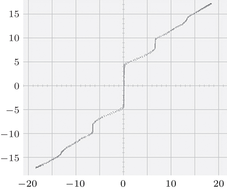 | Fig. 3. AC I– V curve of junctions in series measured at 6.2 K. The horizontal and vertical divisions are 5 mV and 5 mA respectively. The microwave frequency is 6.31 GHz corresponding to a 13-μ V voltage step for each junction. |
Compared with other research results, the critical current is still too large.[7] The zero step is not suppressed enough by the microwave. This may be due to the large critical current which needs large microwave power to drive. Also the transmission of microwave needs to be optimized, for example, by the flip-chip on flex method instead of the bonding technology.[13]
Nb/NbxSi1− x/Nb Josephson junction arrays with different areas are fabricated. The DC and AC I– V characteristic curves are measured and analyzed. Shapiro steps of 500 junctions in series are observed. For junctions with different barriers, critical current density is tuned. The results conform with the results from the tuning method. The junction parameters are optimized by adjusting the NbxSi1− x barrier content to fabricate junctions that are suitable for working in a range between 15 GHz and 20 GHz and integrate more junctions in an array in order to output higher voltage in the future.
The authors would like to thank S. P. Benz, Paul D. Dresselhaus, O. F. Kieler, Gao Yuan, Qu Ji-Feng, Zhao Shi-Ping and Zhu Xiao-Bo for their helpful discussion.
| 1 |
|
| 2 |
|
| 3 |
|
| 4 |
|
| 5 |
|
| 6 |
|
| 7 |
|
| 8 |
|
| 9 |
|
| 10 |
|
| 11 |
|
| 12 |
|
| 13 |
|