Influence of ultra-thin TiN thickness (1.4 nm and 2.4 nm) on positive bias temperature instability (PBTI) of high-

Influence of ultra-thin TiN thickness (1.4 nm and 2.4 nm) on positive bias temperature instability (PBTI) of high- |
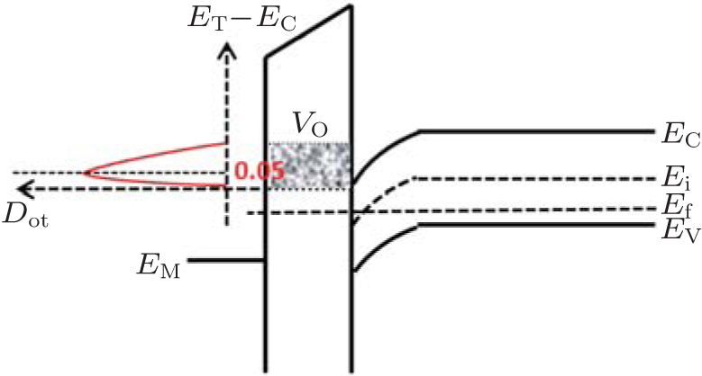
| Band diagram of silicon/high- k /metal gate stacks. The shadow area represents the trap energy range that is strongly influenced by stress and the dot distribution is given. |
 |